High yield
Obtaining a large number of device per wafer is not enough if the process yield is not optimized.
Being Innoscience an IDM and thus controlling the full manufacturing flow (from epitaxy until the transistor completion), Innoscience could improve every technology aspect in order to obtain both high wafer and device yield.
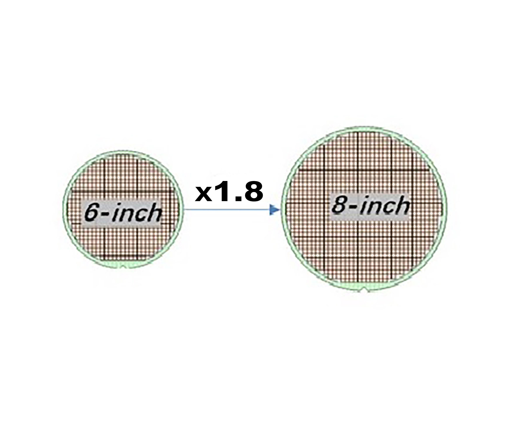
Innoscience has optimized the epitaxy processing in order to obtain uniform, reproducible and robust 8-inch GaN-on-Si epi-wafers, which are the basis for the device processing. Next to this, Innoscience has optimized the process technology, enlarge process windows etc.. in order to obtain a reproducible process and a large number of good device per wafer.
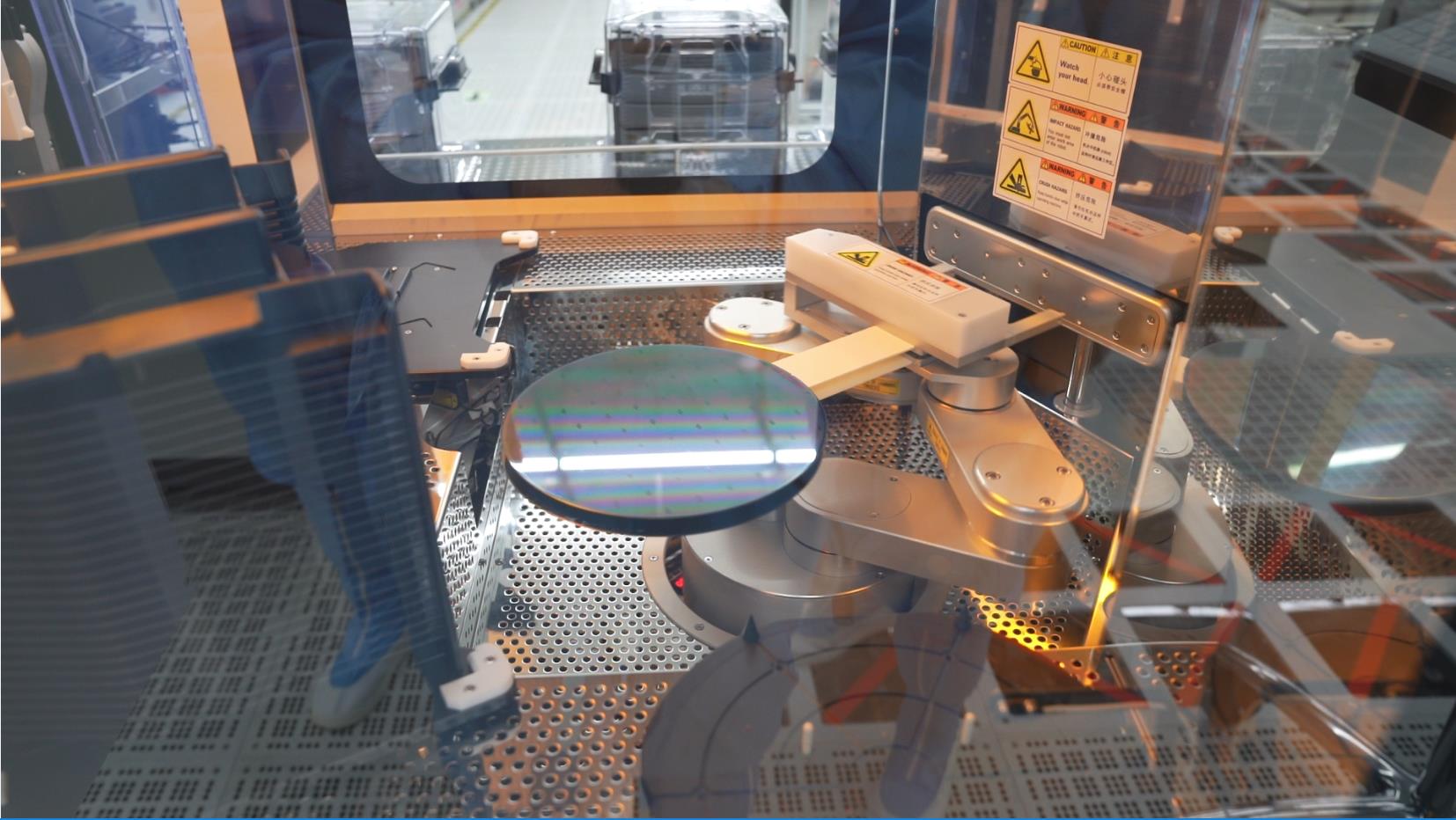
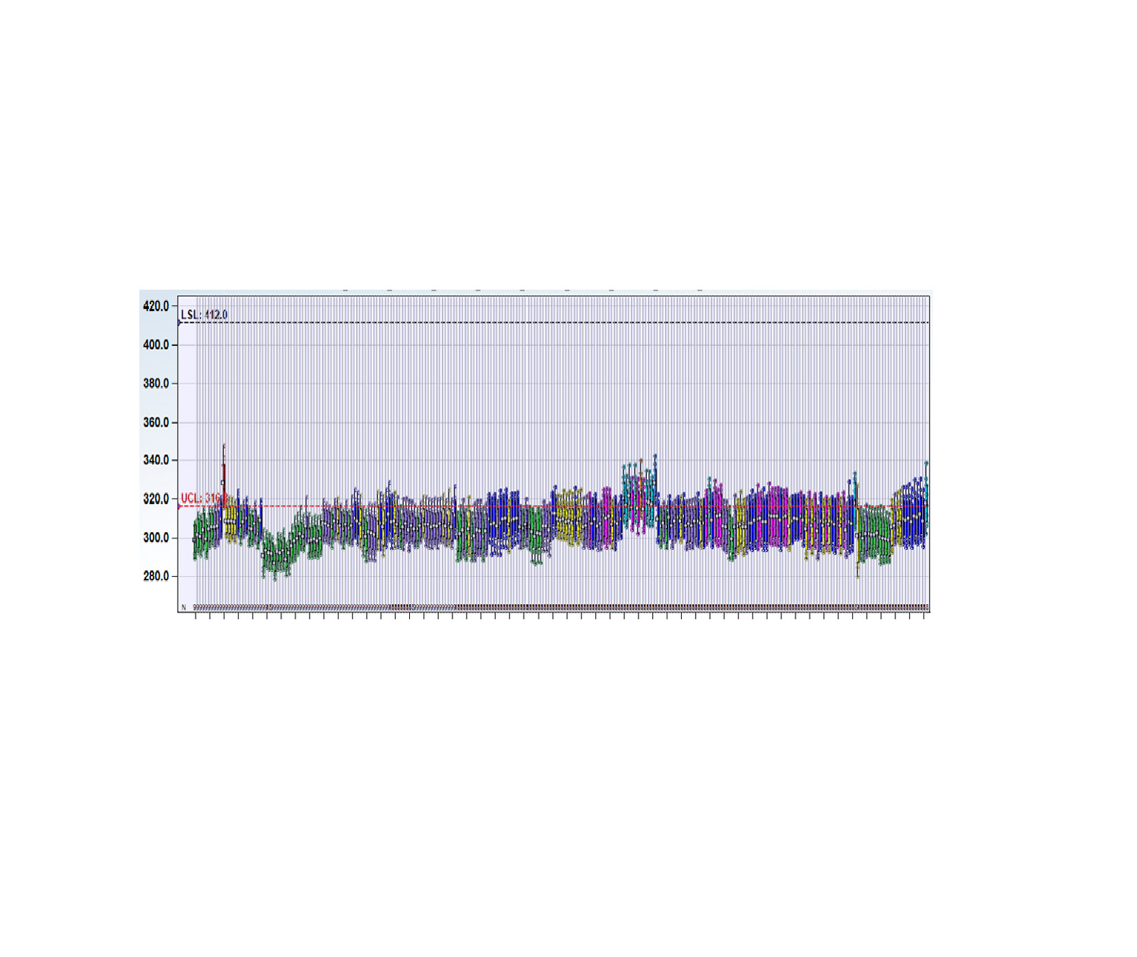
Today, Innoscience has been producing more than 10,000 wafers/month with excellent reproducibility and high wafer and device yield.

 English
 简体
简体