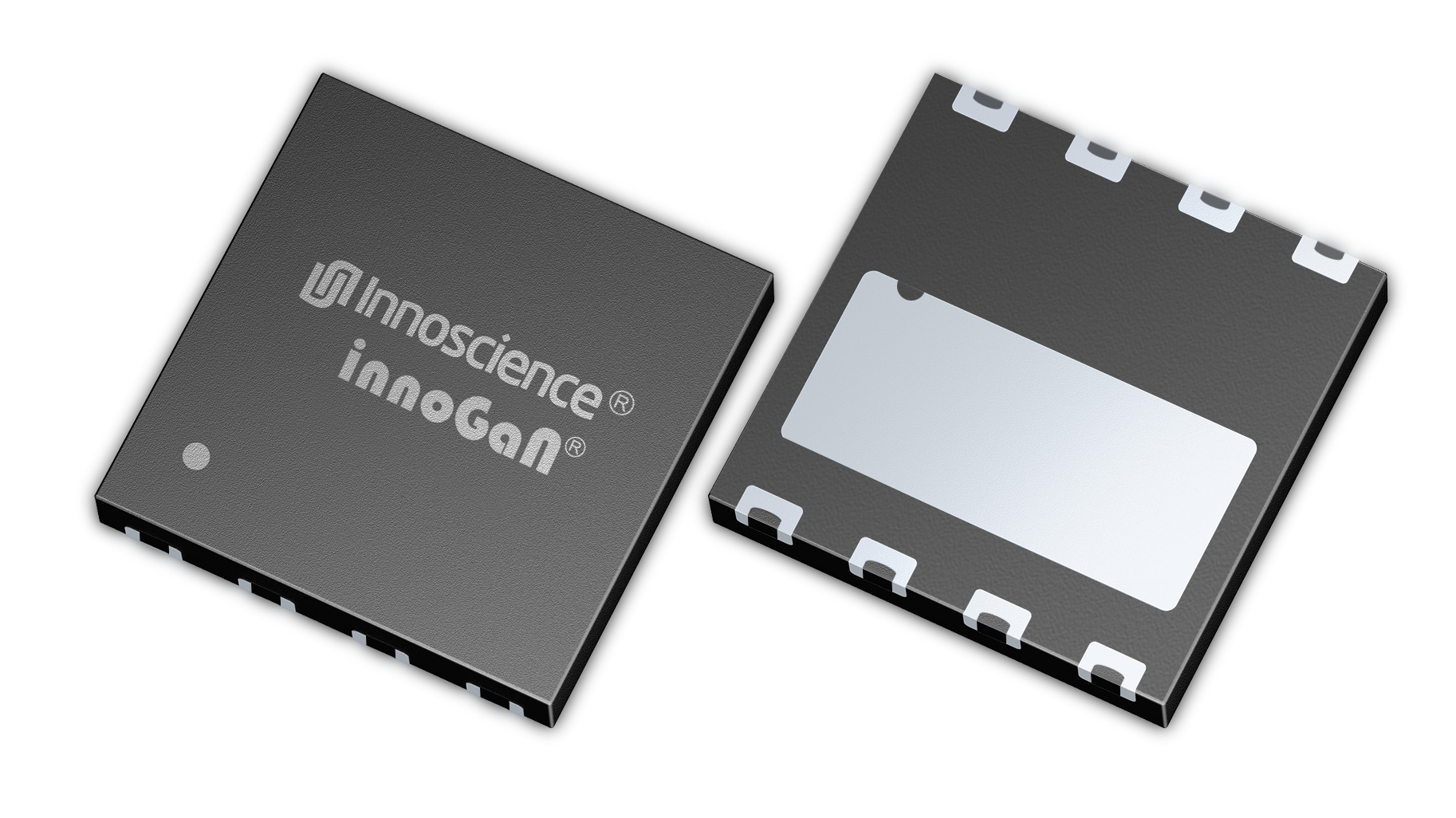
| Platform ( INN650D080BS/INN700D080BS) |
|---|
| Test Items | Test Conditions |
Sample Size
(Unit x Lot)
| #Fail | Result |
|---|
| HTRB |
T=150°C, VDS= 560V, 1000hrs |
77 x 3 |
0 Fail |
Pass |
| HTGB |
T=150°C, VGS= 7V, 1000hrs |
77 x 3 |
0 Fail |
Pass |
| *HTGB(-) |
T=150°C, VGS= -6V, 1000hrs |
77 x 3 |
0 Fail |
Pass |
| TC |
-55 to +150°C, Air, 1000Cys |
77 x 3 |
0 Fail |
Pass |
| HAST |
T=130°C, RH=85%, VDS=100V, 96hrs |
77 x 3 |
0 Fail |
Pass |
| H3TRB |
T=85°C, RH=85%, VDS=560V, 1000hrs |
77 x 3 |
0 Fail |
Pass |
| MSL3 |
T=30°C, RH=60%, 3 x reflow, 192hrs |
25 x 3 |
0 Fail |
Pass |
| HBM |
All Pins |
3 x 1 |
0 Fail |
Class 2 |
| CDM |
All Pins |
3 x 1 |
0 Fail |
Class C3 |
| HTOL (LLC) |
Tj=125°C, Input: 220 Vac, Vout=48V, Vplat=400V, fsw=130KHz |
10 x 3 |
0 Fail |
Pass |
| HTOL(QR-PFC) |
Tj=125°C, Input: 90 Vac, Output: 20V/6.5A, F=120KHz(QR)/100KHz(PFC) |
10 x 3 |
0 Fail |
Pass |
| Note:*HTGB(-)was optional test item for device with bidirectional ESD design. |
|
Spin-off Product
|
|---|
| Test Items | Test Conditions |
Sample Size
(Unit x Lot)
| #Fail | Result |
|---|
| HTRB |
T=150°C, VDS= 560V, 168hrs |
77 x 1 |
0 Fail |
Pass |
| HTGB |
T=150°C, VGS= 7V, 168hrs |
77 x 1 |
0 Fail |
Pass |
| New Package Type Qualification test |
|---|
| Test Items | Test Conditions |
Sample Size
(Unit x Lot)
| #Fail | Result |
|---|
| TC |
-55 to +150°C, Air, 1000Cys |
77 x 3 |
0 Fail |
Pass |
| HAST |
T=130°C, RH=85%, VDS=100V, 96hrs |
77 x 3 |
0 Fail |
Pass |
| H3TRB |
T=85°C, RH=85%, VDS=560V, 1000hrs |
77 x 3 |
0 Fail |
Pass |
| MSL3 |
T=30°C, RH=60%, 3 x reflow, 192hrs |
25 x 3 |
0 Fail |
Pass |
| Note: Package type Spin off have the same package process and design rules |

 English
 简体
简体


