English
 简体
简体

1.1 Features
- GaN-on-Silicon E-mode HEMT technology
- Very low gate charge
- Ultra-low on resistance
- Very small package size
- Zero reverse recovery charge
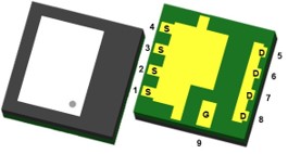
100V Enhancement-mode GaN Power Transistor
GaN-on-Silicon enhancement mode high-electron-mobility-transistor (HEMT) in En-FCLGA with 3.3 mm x 3.3mm package size.
| Spin off Qualification Result | |||||
|---|---|---|---|---|---|
| Note: * Spin off products have same device process and design, H/LTRB, H/LTGB+/, H/LTGB- test refer to INN100EA035A and INN100EBD018DAD. Note: EN-LGA 3.3X3.3 and EN-LGA 5x6 have same package process, EN-LGA 5x6 package reliability refer to EN-LGA 3.3x3.3 (INN100EA035A) and verify 3 lots TC and 1lot package related reliability (MSL3/H3TRB /uHAST/IOL/RSH/Solderability). | |||||
| Test Items | Test Condition | INN100EBD018DAD | INN100EBD025DAD | INN100EBD050DAD | Result |
| HTRB | T=150°C, VD=100V, 168hrs | 77 x 1 | 77 x 1 | 77 x 1 | Pass |
| LTRB | T=-40°C, VD=100V, 168hrs | 77 x 1 | 77 x 1 | 77 x 1 | Pass |
| HTGB | T=150°C, VG=6V, 168hrs | 77 x 1 | 77 x 1 | 77 x 1 | Pass |
| LTGB | T=-40°C, VG=6V, 168hrs | 77 x 1 | 77 x 1 | 77 x 1 | Pass |
| ESD-HBM | T=25°C, All pin | 10 x 1 | 10 x 1 | 10 x 1 | Class_1B |
| ESD-CDM | T=25°C, All pin | 10 x 1 | 10 x 1 | 10 x 1 | Class_C2a |
| MSL3 | T=30°C, RH=60%, 3 x reflow, 192hrs | 25 x 1 | /* | /* | Pass |
| H3TRB | T=85°C, RH=85%, VD=80V, 1000hrs | 77 x 1 | /* | /* | Pass |
| PLTC | -55 to +150°C, Air, 1000Cycles | 77 x 3 | /* | /* | Pass |
| uHAST | T=130°C, RH=85% | 77 x 1 | /* | /* | Pass |
| IOL | ΔTj ≥ 125℃; ton / toff = 1 min /5 min, 5000 Cycles | 77 x 1 | /* | /* | Pass |
| RSH | T=125°C bake 24hrs, T=30°C RH=60% soak 192hrs, | 30 x 1 | /* | /* | Pass |
| 260±5℃, 10±1s | |||||
| Solderability | Precondition Condition C (8hrs), Pb-free:245±5℃, 5±0.5s | 10 x 1 | /* | /* | Pass |
| Parameter | Value |
|---|---|
| VDS,max | 100V |
| RDS(on),typ @ VGS = 5 V | 3.8mΩ |
| RDS(on),max @ VGS = 5 V | 5mΩ |
| QG,typ @ VDS = 50 V | 5.7nC |
| IDS,Pulse (TJ = 25˚C) | 300A |
| QOSS @ VDS = 50 V | 29.7nC |