On November 26th, Innosceience demonstrated its All GaN solutions at the 2021 (Autumn) USB PD & Type-C Asia Expo. At the same time, Zou Yanbo, senior product application manager of Innoscience, delivered a keynote speech on "High-Performance All GaN Solutions Accelerate USB PD 3.1 Application", in which he shared his insights on GaN market value and new application trends!
Zou Yanbo, Senior Product Application Manager of Innoscience
"The USB PD 3.1 fast charging standards bring higher output voltage, higher power and power density. In addition to cell phones, tablets, and laptops, they can also be applied to multiple scenarios such as monitors, cameras, drones, cleaning robots, power tools, and electric bicycles," Zou Yanbo pointed out, "At present, Innoscience's GaN devices can cover all application scenarios."
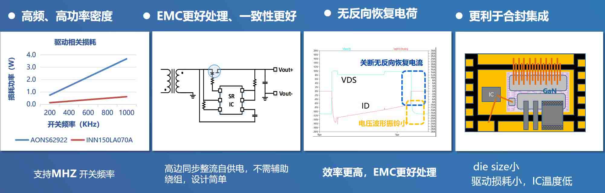
However, the introduction of USB PD 3.1 protocol has also posed new challenges to power supply design. The power devices made of GaN can perfectly respond to the challenges in power supply design by virtue of their outstanding efficiency and high switching frequency.
Therefore, Innoscience has launched a full range of All GaN solutions from 65W to 240W to further improve power density and efficiency. It has launched 150V GaN chips to deliver the All GaN solutions, improving performance by 2-3 times compared with the 150V Si MOS with the highest standard on the market.
According to Zou Yanbo, the following three types of Innoscience’s All GaN solutions are available: 65W1C, 140W 28V/5A and 240W 48V/5A.
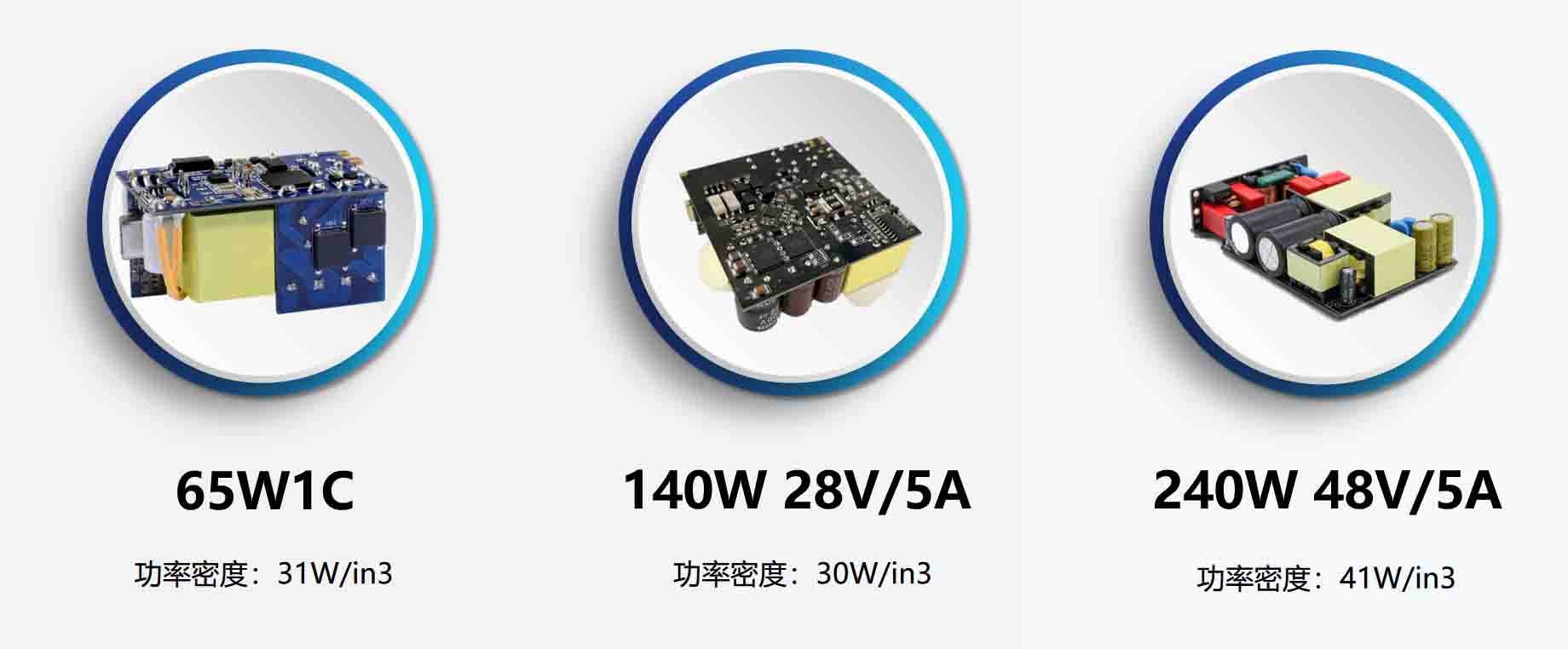
Among them, the power density of the 65W All GaN solution upgraded based on the performance of 150V GaN chips can reach 31W/in3. Its efficiency is 93.4% at 90V AC and 94.7% at 230V.
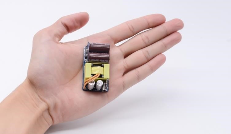
The 140W solution can support 28V/5A output with a bridgeless PFC+ACF architecture and a power density of 30W/in3, with a size comparable to a traditional 65W fast charger.
The 240W (PD3.1 48V5A) solution adopts the Totem-pole bridgeless PFC+LLC design, with a power density of 41W/in3 and a size of a bank card.
According to Zou Yanbo, while mass producing high and low voltage GaN devices, Innoscience is also committed to delivering full-link, high-efficiency, high-frequency and high-density solutions, and moving from the front-end grid side to chargers and to the interior of cell phones, to delivery end-to-end solutions and help improve energy efficiency. It is worth mentioning that with the help of the IDM model, Innoscience can increase the number of chips on a single wafer by about two times with every two generations of product upgrades.
Thanks to the rich InnoGaN series product line, Innoscience is racing ahead in the consumer power market. With a current shipment that exceeds 40 million units, Innoscience has delivered solutions for many famous brands and manufacturers including Lenovo, Nubia, Meizu, ANKER, UGREEN, Baseus, Pisen, MOMAX, ROCK, REMAX, QCY, Lapo, and tagic, and launched exceptional GaN application solutions together with partners.
Looking into the future, Zou Yanbo said that All GaN solutions will have extensive application opportunities in four major fields, namely green energy, data center energy, intelligent electric power and DC buildings. "Innoscience is doing something meaningful with “GaN”. If GaN is used to improve the efficiency of the whole power supply circuit by 5%, it can reduce 1 billion tons of carbon emissions assuming a global annual power consumption of 27 trillion kWh."
Overall, as the world's first company to mass produce 8-inch GaN-on-Si chips, Innoscience is leading the global development of the third-generation semiconductors with its surging sales. With the successful mass production of Innoscience's Suzhou plant, it is also well prepared to fully embrace the coming golden era of GaN.
The link: https://laoyaoba.com/n/799609

 English
 简体
简体
