World's largest 8-inch GaN-World's largest 8-inch GaN-on-Si device maker presents performance and reliability data of 15V and 650V GaN power device at prestigious IEEE conferenceon-Si device maker presents performance and reliability data of 15V and 650V GaN power device at prestigious IEEE conference
May 20, 2022 – Innoscience Technology, a company founded to create a global energy ecosystem based on high-performance, low-cost gallium-nitride-on-silicon (GaN-on-Si) power solutions, will present two papers at the prestigious IEEE International Symposium on Power Semiconductor Devices (ISPSD) conference in Vancouver, Canada, May 22-25.
The first paper systematically evaluates the reliability and switching lifetime of a 650-V commercial GaN-on-Si HEMT fabricated on a 200mm (8-inch) CMOS-compatible process platform for a high-density PFC Boost power converter application. Innoscience’s engineers shows that by adopting Innoscience’s Strain Enhancement Layer (SEL) technology, a stable Dynamic RDS(on) (< 1.2x) during the 1000-hrs switching stress test is achieved, which is further confirmed by the wafer-level stress system. Device without SEL layer, on the contrary, shows a quicker degradation of the Dynamic RDS(on) that increases 18 times during the first 3 hours of stress. By performing Emission Microscope (EMMI) to detect the electroluminescence of device in situ during switching stress, scientists at Innoscience has highlighted that the SEL suppressed the hot carrier injection, which is believed to contribute to the increase of the Dynamic RDS(on) on samples without SEL technology.From the switching acceleration test, a lifetime up to 29 years was achieved, which satisfies the requirements in the industrial applications.
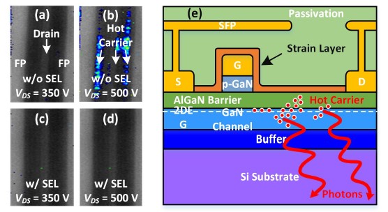
Hot carrier photoemission for device w/o SEL (a) 350 V, (b) 500 V, and w/ SEL (c) 350 V, (d) 500 V. (e) Device cross-section shows the hot carrier location and photoemission.
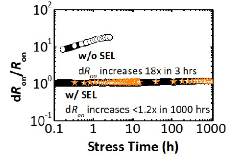
Comparison of dRon without and with the SEL under the hard switching test with Vds = 600 V, Vgs = 6 V, and fs = 100 kHz.
The second paper is titled 'Dynamic RDS(on) and Vth free 15 V E-mode GaN HEMT delivering low switching Figure of Merit (sFOM) of 13.1 mΩ·nC and over'. The power devices discussed achieve record-low sFOM on commercialized 200 mm GaN-on-Si platform made for mass production.Although tremendous efforts have been made in low voltage GaN HEMT for consumer electronics, where power switches are typically below 40 V, the wide adoption of low voltage GaN HEMT still faces huge challenge as compared with its silicon counterpart as the contact resistance or parasitic capacitance proportion rises up as dimensions shrink down, the threshold voltage Vth decreases and the risk of false turn-on increases, off-state leakage current increases and results in large quiescent loss and long-term static and dynamic instability. All these issues hinder the wide acceptance of low voltage GaN HEMT in volume constrained portable electronics.
Innoscience shows that their InnoGaN withstands 1000 hours’ continual stress over wide temperature range with minimum parametric shift and continuous-switching stress in both hard-/soft-switching mode with negligible dynamic Ron and Vth shift. Device performance is further validated in buck converter with GaN HEMTs in half bridge configuration and demonstrates superior efficiency over 80% at tens of MHz. Thus, InnoGaN HEMTs rated for 15V unlocks the full potential of GaN power switches targeting for fast-speed high-frequency buck converter in tens of MHz with peak efficiency 90% with long-term system dynamic stability.
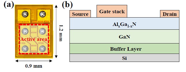 (a) Optical microscopy of the 15 V GaN HEMT in wafer-level chip-scale package (WLCSP) with few pH parasitic inductance. (b) Cross-section of the fabricated GaN HEMT.
Dr Denis Marcon, General Manager, Innoscience Europe comments: "The two papers are highly detailed and include comprehensive test data as befits submissions to this industry-recognized, important IEEE conference. We hope that attendees will understand that Innoscience is clearly the leader in GaN devices produced on 8-inch silicon wafers, with fully-characterised performance and reliability data both for Low Voltage (LV) and High Voltage (HV) devices."
The link: https://www.eeworldonline.com/technical-papers-demonstrate-15-v-and-650-v-gan-power-device-performance-and-reliability-data/
– Ends –
About Innoscience
Innoscience is an Integrated Device Manufacturer (IDM) founded in December 2015 with investment from venture capitals from the world. With the development of new technologies, the electric power grid and power electronic systems across the world are undergoing a massive transformation. Our vision is to create an energy ecosystem with effective and low-cost Gallium-Nitride-on-Silicon (GaN-on-Si) power solutions. In November 2017, Innoscience first established a mass production 8-inch wafer line for GaN-on-Si devices. As a cutting-edge GaN technology provider, Innoscience’s 1,400+ employees and over 300 R&D experts are dedicated to delivering high performance and high reliability GaN power devices that can be widely used in diverse applications including cloud computing, electric vehicles (EV) and automotive, portable devices, mobile phones, chargers and adapters. For more information, please visit www.innoscience.com.
Contact Media:
Peter Rogerson, Innoscience
peterrogerson@innoscience.com
+1 408-502-4626
Benoit Simoneau, 514 Media
benoit@514-media.com
+44 (0) 7891 920 370
Contact Media:
Ian Wood, WPG EMEA
ian.wood@wpgemea.com
+44 1628 958 394

 English
 简体
简体
