ijiwei. com On December 20 - 21, the 16th "China Chip" Conference on Promotion of China IC Industry 2021 and the Launch Ceremony of "China Chip" Excellent Product Selection Event was held in Zhuhai. At the Summit on Achieving Carbon Neutrality with Wide Bandgap Semiconductors on the 21December, Mr. Wang Huaifeng, Vice General Manager of Innoscience Technology Co., Ltd (Innoscience), delivered an excellent speech on "A Gift to the Green Earth - GaN".
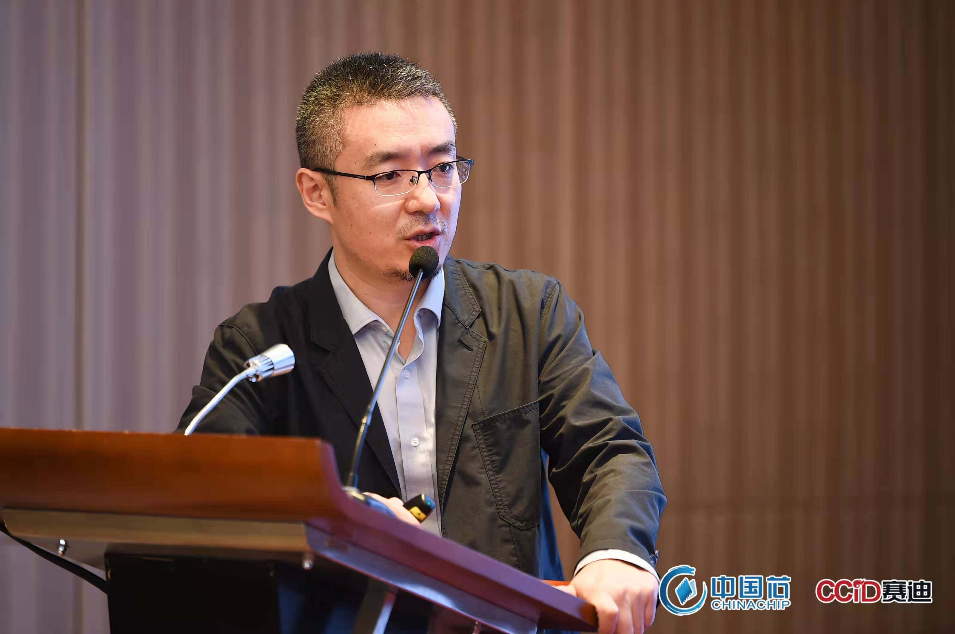
Wang Huaifeng, Vice General Manager of Innoscience
GaN power devices: improving system efficiency and reducing power loss
At the summit, Wang Huaifeng pointed out that "there have been four industrial revolutions, and we are in the middle of the fourth one, which is digitalization. This industrial revolution features artificial intelligence, 5G, smart driving, green energy, among others".
In the digital era, we use intelligent terminals (ends) to interconnect everything through high-speed communications (pipes) and data centers (clouds). At the same time, new application scenarios, such as Al, big data, data processing centers, electric vehicles and autonomous driving, have emerged.
According to Wang Huaifeng, "The emergence of these new application scenarios will lead to a dramatic increase in global electricity demand, which will grow by more than 50% by 2030 compared to 2020. Where there is electricity, there is a need for conversion. Therefore, more power devices will be needed to drive industrial development in the future."
What’s more, the dramatic increase in electricity demand will also lead to increased energy consumption, which goes against the eco-friendly goals of carbon peaking and carbon neutrality.
"Reducing power loss while using electricity is the key to reducing CO2 emissions. According to statistics, 5G applications will consume 70% more power than 4G applications. It is estimated that global data centers will account for 18% of the total global energy consumption by 2025. Therefore, reducing emissions in the face of higher electricity demand means there’s a higher request for bringing down power loss in the conversion process," said Wang Huaifeng.
Industries in the digital era are eco-friendly, efficient and intelligent, which means there’s a pressing need for higher power efficiency and component reduction to minimize power loss.
Wang Huaifeng believes that power losses in the conversion process is completely wasteful, and silicon power devices are unable to meet our current emissions standards. GaN’s promising advantages of high switching frequency, low on-resistance, small size and multiple functions mean that GaN power devices have higher system efficiency, less power loss, compact shape and more simplified system design. GaN chips can offer significantly improved performance and greatly reduce energy consumption with a much smaller size, which can facilitate emission reduction.
In addition, the emergence of GaN may improve device performance exponentially, bringing huge system advantages to industrial applications. "Power devices are a universal device. Where there is electricity, there are power chips, though with different forms. Different application scenarios have different requirements for power devices. GaN power devices can contribute to greater performance in various scenarios including consumer, industrial, and automotive sectors," said Wang Huaifeng.
GaN is a gift for the green earth
With new opportunities come intensifying global competition. Since 2009, when the first EPC 100V power GaN FET was launched to the market, both the shipments of high-voltage and low-voltage GaN chips have reached tens of millions. The sophisticated industrial technology and soaring market demand have given rise to a number of global GaN mainstream players - Innoscience tops among them.
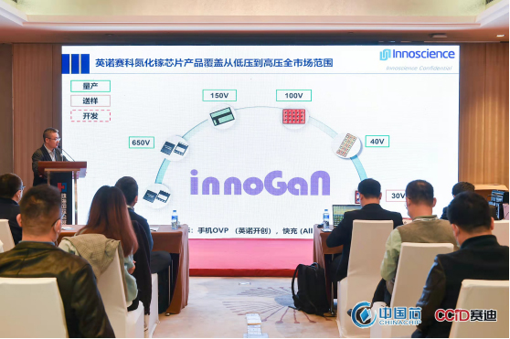
According to Wang Huaifeng, "Innoscience was established in December 2015. Its Zhuhai production line was put into operation in November 2017. In 2019, it began to mass produce low-voltage and high-voltage GaN devices for shipments. The year 2021 marks the first year of Innoscience’s new journey. Its Suzhou factor has been put into production. There has been a significant increase in shipments of its high-voltage and low-voltage chips. The total shipment of more than 40 million chips indicates Innoscience’s sophisticated mass production technology."
What's worth mentioning is that Innoscience adopts the IDM business model, which is a production model that integrates chip design, epitaxial growth, chip manufacturing, reliability and failure analysis and involves the entire industrial chain. The use of 8-inch GaN-on-Si indicates absolute competitive advantages in product cost and price. Meanwhile, Innoscience also has sophisticated reliability and failure analysis platforms to facilitate faster product iteration. In addition, Innoscience is the world’s only GaN company that has an advanced ASML lithography manufacturing process, which gives it a significant advantage over its global competitors. At present, Innoscience can produce 10,000 wafers of 8-inch GaN chips per month, with a voltage range of 30~650V.
The emergence of new things follows the laws of development. To be specific, a new product starts with the more receptive markets, and then gradually moves to penetrate the high-end market. The same law applies to GaN. There has been two mature GaN ecosystems as the industrial technology gets more sophisticated. Wang Huaifeng pointed out that one ecosystem is fast charging, the pioneer market of GaN application. The fast charging market is a relatively mature market with a good number of competing players. The other ecosystem is the OVP application of cell phones. At present, Innoscience’s GaN chips have covered both ecosystems.
In addition to the two mature ecosystems, GaN also focuses on application scenarios including data center power supply and new energy vehicles.
In terms of data center power supply, GaN can address the bottleneck of large ASIC chips. For example, it can effectively meet the requirement of data centers’ GPU for high current (which is more than 1000A). GaN’s high frequency advantage can effectively reduce the area of power supply system and realize high power density power supply. Data centers using GaN are more energy-efficient. It is estimated that the annual power saving of one cabinet is equivalent to a reduction of about 8 tons of CO2 emissions. This is an outstanding contribution when calculated based on data centers’ 18% share of the total energy consumption.
When it comes to the application of GaN in new energy vehicles, Wang Huaifeng said that GaN is a solution for LiDAR, since both Si and SiC fail to address its requirements for high switching speed. LiDAR is GaN’s first application scenario in the automotive field. Other application scenarios also include DC-DC, on-board charger, among others.
Wang Huaifeng believes that GaN is a gift to the green earth, and it’s still in its infancy. The entire industrial chain need to work together to make this small tree grow taller.
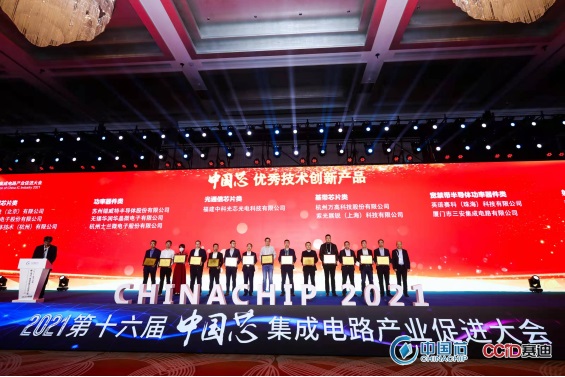
It is worth mentioning that in the "China Chip" selection event, Innoscience’s high-voltage GaN HEMT/INN650DA260A stood out and won the title of "Excellent Technology Innovation Product".
The link: https://www.laoyaoba.com/html/share/news?source=app_android_v71&news_id=802187&fromShare=android&utm_source=utm_source_sharewxf

 English
 简体
简体
