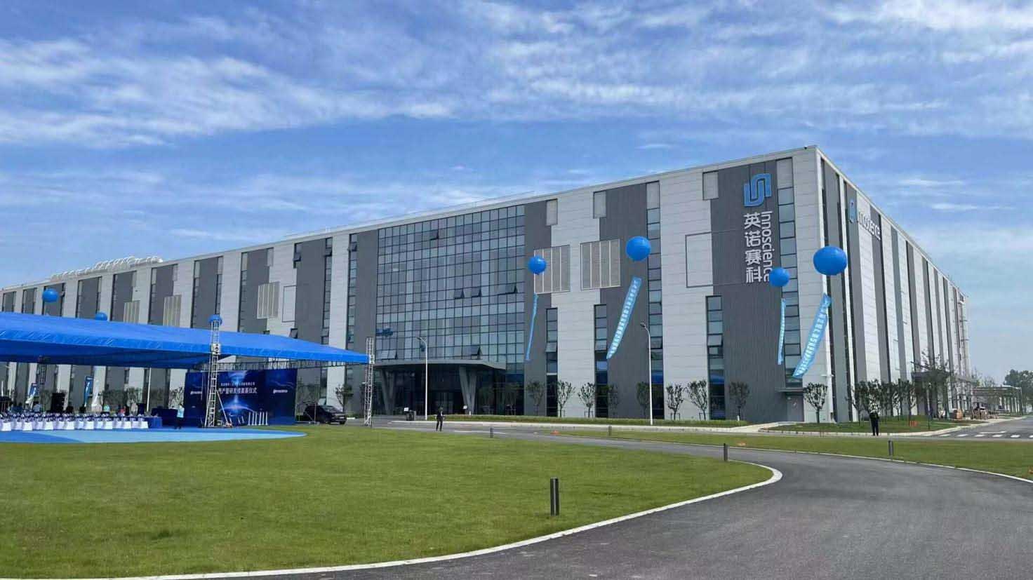
ijiwei. com Innoscience (Suzhou) Semiconductor Co., Ltd. held a mass production and R&D building groundbreaking ceremony in Fenhu Hi-tech Development Zone on June 5. The estimated investment of the first phase of the project is 8 billion RMB. Plant construction and equipment relocation were completed in 2020, and the mass production will start immediately, making Innosceince the first company in the world to mass produce GaN chips on 8-inch silicon substrates. With incrementally increased production capacity, 6,000 wafers per month can be produced by the end of 2021. By the end of 2022, the Suzhou plant will have an annual capacity of 780,000 wafers of 8-inch GaN-on-Si, with an estimated output value of 15 billion RMB per year and a profit and tax of 1.5 billion RMB.
Hua Yuan, Deputy Secretary General of Shanghai Municipal Government, Director of the Shanghai Development and Reform Commission, Director of the Executive Committee of the Yangtze River Delta Integration Demonstration Zone, Luo Weiwei, Chairman of Innoscience, Shen Guofang, Deputy Director of the Standing Committee of the Suzhou Municipal People's Congress, Li Ming, Party Secretary of Wujiang District Committee, Ding Wenwu, President of National Integrated Circuit Industry Investment Fund, Tang Xiaodong, Deputy Director of the Executive Committee of the Yangtze River Delta Integration Demonstration Zone and Deputy Director of Jiangsu Development and Reform Commission, Wan Li, Director of Suzhou Bureau of Industry and Information Technology, Sun Zaiheng, General Manager of Innoscience, Zhang Binggao, Member of the Standing Committee of Wujiang District, Party Secretary of the Working Committee and Director of the Management Committee of Fenhu Hi-tech Development Zone, Wu Ling, Chairman of the Third-Generation Semiconductor Industry Technology Innovation Strategic Alliance, Qian Yu, member of the Standing Committee and Deputy Mayor of Wujiang District, Wu Zuoyi, President of SK Group Greater China, and Wang Hongbo, Chief Investment Officer of CMB International, jointly inaugurated the mass production ceremony. The booming sound of cannons and splendid fireworks heralds the new stage of development for Innoscience.
The mass production of GaN-based materials means that the company has entered the fast lane, and R&D is the foundation for Innoscience to move forward. Along with the mass production ceremony, the signing ceremony of the First Phase of the Capacity Expansion Project of the 8-Inch GaN-on-Si Chip Production Line Phase I and the groundbreaking ceremony of the R&D building were also held. Four national ministries and commissions (Development and Reform Commission, Ministry of Industry and Information Technology, Ministry of Finance, and General Administration of Customs) has considered Innoscience as key target of support to manufacture 0.25 micron and below chips thanks to its strong research capabilities and advanced technologies. Innoscience is also the first third-generation semiconductor project in China to follow window guidance from the National Development and Reform Commission. Meanwhile, as a unicorn incubator in Suzhou, Innoscience has undertaken a number of key R&D projects from relevant national ministries and provincial departments. The groundbreaking of the R&D building indicates that more innovations will come into being here in the future.
.jpg)
SON JAYHYUNG, General Manager of Innoscience, pointed out that after more than 7 decades of development, silicon is reaching its limit, while GaN is a potential material for future industrial development. Over the past two years, GaN-based market applications have made many breakthroughs and started to penetrate in the consumer electronics, industrial and automotive markets. In particular, GaN demonstrates huge potential in fields such as fast charging, LIDAR, cell phones, 5G, new energy vehicles, wireless charging and data centers. “I’m confident that GaN-based applications will be the fastest growing sector in the semiconductor industry for the following decade,” Sun Zaiheng emphasized, “Now that Innoscience’s Suzhou plant is ready for mass production, we are fully prepared to embrace the GaN era.”
Wang Hongbo, Chief Investment Officer of China Merchants Bank International (CMBI), said that as the world's first company to build a GaN IDM mass production line, Innoscience has changed and led the global development of the third-generation semiconductors with its milestone breakthrough. He believed that the significance and value of GaN will be tapped into in the future. “As the earliest investor of Innoscience, CMBI made its first investment decision over a Power Point presentation. As an investor managing a wealth pool worth of 100 billion RMB, our value is not about accumulating wealth shrewdly, but about allocating resources to the best entrepreneurs, and change the world together with them.” Wang Hongbo pointed out, “The successful mass production is a proud moment for us, and we’re also grateful to the government and upstream and downstream partners who have given us strong support during our investment in Innoscience. The development of the third-generation semiconductor industry has just begun, and it is important that all partners of the industry work together to develop an ecosystem and create a better future.”
Wu Ling, Director of the Third-Generation Semiconductor Industry Technology Innovation Strategic Alliance, said that China's solemn commitment to carbon peak and carbon neutral and the establishment of a new power system that features new energy sources mean that the third-generation semiconductor industry can unleash huge market potential and strong development momentum. “Innoscience’s mass production of 8-inch GaN-on-Si is at the forefront of the world, but China still has a long way to go before its compound semiconductors, especially the third-generation semiconductors, can take the lead. There is still a huge gap between China and the world’s major players when it comes to future disruptive technologies such as power semiconductors including silicon carbide and substrates. Also, improvements need to be made in the R&D system and industrial ecosystem.” Wu Ling stressed that “the 14th Five-Year Plan clearly puts forward key development fields such as integrated circuits, silicon carbide and gallium nitride. It is expected that Innoscience will play a leading role in the future to drive industrial development and contribute to the green and low-carbon sustainable development of mankind and help create a better life in the future."
Founded in October 2017 with a registered capital of 2.7 billion RMB, Innoscience (Suzhou) Semiconductor Co., Ltd. is a high-tech company committed to the R&D and industrialization of third-generation semiconductor GaN-on-Si. The company adopts the IDM full industry chain model, which integrates chip design, epitaxial growth, chip manufacturing, testing and failure analysis. It manufactures a series of products covering 30-900V power semiconductor devices, IC and RF devices, and is the only company in the world that can mass produce both low-voltage and high-voltage GaN-on-Si chips. So far, Innoscience has more than 1,000 employees and more than 500 domestic and international core patent applications.
The link: https://laoyaoba.com/n/782840

 English
 简体
简体
