Thanks to the popular application of GaN devices with high frequency and efficiency, switching loss has been reduced and switching frequency has been increased. The GaN technology has also increased the conversion efficiency of power supplies significantly and reduced the size of USB PD fast chargers by half compared with conventional fast chargers with the same power. At the same time, GaN can be used not only in USB PD fast charging, but also in many high-power conversion applications. The technology can also be used in laptop power supplies or multi-port fast chargers to reduce heat generation and size.
Innoscience joined hands with NXP and developed a 150w GaN power supply solution, which uses a full set of NXP's controllers and Innoscience’s GaN power devices-mounted PFC and LLC transistor switches, with an output voltage of 21.5V. It can be used for laptop power supply or independent step-down multi-port USB PD fast chargers. The power solution is only 65*55*22mm in size, with a power density of 1.9W/cm³ and over 95% efficiency.
This 150W GaN-based switching power supply adopts the PFC+LLC circuit architecture, which is indicated in the reference design. It supports 90-264V AC input and has less than 80mW of standby power consumption under no load conditions. A full set of NXP controller solutions are adopted inside. The active bridge rectifier, 2-in-1 combo controller and synchronous rectifier controller are all from NXP, and the PFC boost switch and LLC switch use GaN switch devices from Innoscience.
According to the reference design, the full-load output efficiency of this power supply is above 94% at 115Vac input and above 95% at 230Vac input. The input power loss is less than 100mW at 230Vac under no load conditions.
1. Referenced appearance of the 150W GaN power supply
.jpg)
As seen from the front, four small boards are vertically welded to the large board to increase the available board area and improve space utilization. The four small boards are the active bridge rectifier, PFC transistor switch, LLC transistor switch and synchronous rectifier, which are interspersed between the PFC boost converter and the LLC transformer.
.jpg)
The circuit components of this power supply are quite simplified due to the use of multiple small boards and NXP’s highly integrated PFC+LLC 2-in-1 controller, which significantly streamline the debugging and production process of the power solution.
.jpg)
The length of the circuit board is about 65mm when measured with a vernier caliper.
.jpg)
The width of the circuit board is about 55mm when measured with a vernier caliper.

The height of the circuit board is about 19.32mm when measured with a vernier caliper.
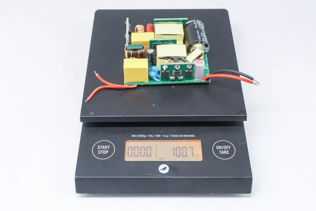
It weighs 100.7g.
2. Circuit analysis of the 150W GaN power supply
This power supply uses active rectification in its primary design to reduce the loss caused by rectifier voltage drop. The full set of NXP power supply solution that features TEA2206T active rectifier controller + TEA2017AAT PFC + LLC controller + TEA2095T synchronous rectifier controller is adopted, with Innoscience’s new INN650DA260A GaN device and the DFN5*6 package, to deliver a high-performance and small-sized 150W switching power supply design.
The switching power supply input is designed with an active bridge rectifier to reduce the losses caused by rectifier voltage drop. In addition, it doesn’t require cooling solutions as traditional bridge rectifiers do, thus making the design more compact.
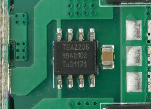
NXP’s TEA2206T is an active bridge rectifier controller for replacing the two low-side diodes in the traditional diode bridge with MOSFETs. Using the TEA2206T with low-ohmic high-voltage external MOSFETs significantly improves the efficiency of the power converter as the typical rectifier-diode forward-conduction losses are reduced by 50%.
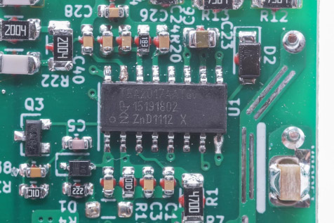
Inside the power supply is the NXP TEA2017 controller, a 2-in-1 controller that integrates a multi-mode PFC and a digitally configured LLC. The integration of two chips means that the controller can output both PFC and LLC drive signals without the need for two separate chips as the conventional design does.
The TEA2017AAT is a digital configurable LLC and PFC combo controller for high-efficiency resonant power supplies. It includes both the LLC controller and PFC controller functionality. The PFC can be configured to operate in DCM/QR, CCM fixed frequency, or multimode which supports all operation modes to optimize the PFC efficiency. The TEA2017AAT enables building a complete resonant power supply which is easy to design and has a very low component count. The TEA2017AAT comes in a low profile and narrow body-width SO16 package.
The TEA2017AAT digital architecture is based on a high-speed configurable hardware state machine ensuring very reliable real-time performance. During the power supply development, many operation and protection settings of the LLC and PFC controller can be adjusted by loading new settings into the device to meet specific application requirements. The configurations can be fully secured to prevent unauthorized copying of the proprietary TEA2017AAT configuration content.
In contrast to traditional resonant topologies, the TEA2017AAT shows a very high efficiency at low loads due to the LLC low-power mode. This mode operates in the power region between continuous switching (also called high-power mode) and burst mode.
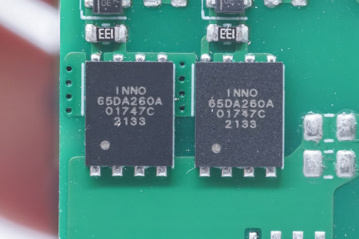
The PFC boost transistor switches are connected in parallel with two Innscience INN650DA260A.

The LLC transistor switch is a half-bridge structure using two wafers of Innoscience INN650DA260A. Both the PFC transistor switch and the LLC transistor switch are controlled by the TEA2017AAT.

The INN650DA260A is a pressureproof 650V GaN-on-Silicon enhancement-mode power transistor that comes in a DFN5*6 package, with a transient voltage reaching up to 800V. Supporting ultra-high switching frequency, it has no reverse recovery charge and has extremely low gate charge and output charge. It is qualified for industrial applications according to the JEDEC Standards, equipped with built-in ESD protection, and complies with the RoHS, lead-free, EU REACH regulations.
The INN650DA260A has a typical resistance of 260mΩ. It supports Kelvin source, has a gate drive voltage of 6V and a breakdown voltage reaching 7V, can withstand pulses from -20V to 10V. It can be used for 65-120W adapters with a flyback architecture and 120-200W adaptors with a PFC and LLC architecture.

The secondary-side synchronous rectifier controller uses NXP TEA2095T for synchronous rectifier control. It is equipped with two built-in drives that can drive two synchronous rectifier transistors simultaneously and support independent operation.

The TEA2095T/TE is a high-performance synchronous rectifier (SR) controller IC for switch-mode power supplies. The synchronous rectifier controller adopts an adaptive gate driver technique to maximize energy savings at any load and improve light-load efficiency. The TEA2095T/TE can operate at a regulated voltage level of -25 mV at 90 μA, which works perfectly with MOSFETs that have low on- resistance.
The combination of NXP’s highly integrated power supply solution and Innoscience’s GaN devices has maximized the performance of both solutions and ensured a compact, reliable and highly efficient switching power supply design. The active bridge rectifier reduces the conduction losses of traditional bridge rectifiers by half, thereby streamlining the cooling design of the bridge rectifier. The use of LLC topology can effectively reduce the switching losses of primary transistor switches and improve conversion efficiency. A synchronous rectifier is used for output to effectively reduce voltage drop and energy loss, which is a problem with traditional diodes. With the compact power supply design, an efficient and small-sized GaN power supply solution design is realized.
NXP is a leading integrated semiconductor company with a wide range of product applications covering markets and fields such as safe and connected vehicles, mobile devices, industrial IoT, smart cities, smart homes, and communications infrastructure. NXP is best known for its commitment to innovation for safe and connected applications in the automotive sector. It also has an extensive portfolio of chips. All of the controller solutions for the power reference design presented here are from NXP Semiconductors.
Innoscience is a world’s leading GaN-on-Si IDM company with a current shipment exceeding 40 million units, of which the high-voltage devices for fast charging have been adopted by hundreds of products of multiple famous brands and manufacturers, such as Lenovo, Nubia, Meizu, ANKER, UGREEN, Baseus, Pisen, MOMAX, ROCK, REMAX, QCY, Lapo, and tegic, indicating a strong market prospect.
With the universal use of GaN for cell phone fast charging, the potential of the high-frequency and high-efficiency GaN technology has been fully unleashed. Innoscience introduces the GaN technology into fixed voltage adapters to meet the needs of laptop and electric bicycle charging. The products are easy to carry around due to their smaller sizes.
With the universal use of GaN for cell phone fast charging, the potential of the high-frequency and high-efficiency GaN technology has been fully unleashed. Innoscience introduces the GaN technology into fixed voltage adapters to meet the needs of laptop and electric bicycle charging. The products are easy to carry around due to their smaller sizes.
The link: https://laoyaoba.com/n/799136

 English
 简体
简体
