2 hours, 1 hour, half an hour, 15 minutes ... the charging speed of cell phones, “companion of mankind”, constantly break the limit in just a few years. The term of gallium nitride has also been frequently mentioned during this process. In fact, fast charging technology now offers near perfect experience thanks to the rapid progress of the third-generation of semiconductor technology represented by gallium nitride (GaN).
According to an industry report published by Nomura in March, third-generation semiconductors will reshape the global power market in the next 2-3 years, replacing power devices made of silicon. Nomura also predicts that in 2023, the market value of third-generation semiconductors will grow at an annual rate of more than 60%. Under such trend, the third-generation of semiconductor competition heats up as major manufacturers are rushing into the market. Who will stand out amongst the competing players? Innoscience is perhaps the most promising seeded player.
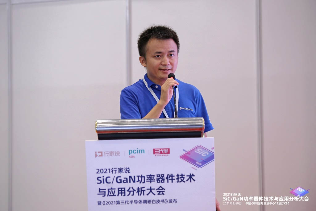
The PCIM Asia 2021 conference was held on September 9 as scheduled, and in the session of SiC and GaN Technology and Application Analysis Conference, Chen Yulin, vice president of product application of Innoscience, delivered a keynote speech titled "All-GaN series solution and its application trend", which was built upon the expansion of the output range of USB PD3.0 as a result of the USB PD3.1 protocol.
With increased battery capacity and better fast charging user experience, high power chargers are developing rapidly; while the power increases significantly, consumers show a preference for smaller chargers, which can only be met by providing higher power density devices. In addition, the expansion of USB PD3.1 protocol also presents new challenges to power supply design. Power switches made of gallium nitride (GaN)/silicon carbide and other wide bandgap materials have unfolded a new era of power electronics with their outstanding efficiency and high switching frequency.
Therefore, Innoscience has launched a full range of All-GaN solutions covering power from 65W to 240W, with improved power density and efficiency.
According to Chen Yulin, there are three types of Innoscience All-GaN solutions: 65W 2C1A, 120W single C and 240W 48V/5A.
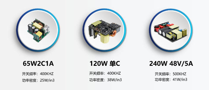
Among them, the 65W solution adopts the ACF+BUCK architecture, with power density of 25W/in3, and a size close to a traditional Si 30W fast charger.
The 120W solution adopts the Boost PFC+ACF architecture, with power density of 38W/in3 and a size comparable to a traditional 65W fast charger.
The 240W (PD3.1 48V5A) solution adopts the Totem-pole bridgeless PFC+LLC design, with a power density of 41W/in3 and a size of a bank card.
Innoscience launched 150V GaN chips to deliver the All GaN solutions. Compared with the 150V Si MOS with the highest standard on the market, Ron*Qg is 6 times smaller, Ron*Coss 2.4 times, and Ron*Area 2.5 times, and the comprehensive performance can be improved by 2-3 times. It has major four advantages: high frequency, high-side self-driven synchronous rectification, no reverse recovery charge, and can better facilitate envelope tracking and integration.
Thanks to the rich InnoGaN series product line, Innoscience is racing ahead in the consumer power market. With a current shipment that exceeds 30 million units, Innoscience has provided advanced GaN solutions for more than 60 clients including Lenovo, Nubia, Pisen, MOMAX and QCY, and launched exceptional GaN application solutions together with partners.
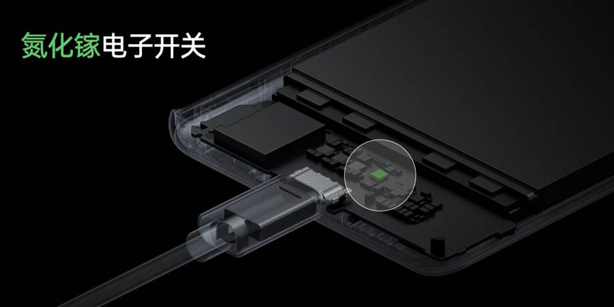
Looking into the future, Chen Yulin said that All GaN solutions will have opportunities for extensive application in three major fields: consumer, data center and electric vehicle. He also revealed that in OPPO’s latest generation of smartphone model, which was launched not long ago, GaN bidirectional switch devices are used in its built-in GaN electronic switches.
As the world's first company that is capable of mass producing 8-inch GaN-on-Si, Innoscience is changing and leading the global development of third-generation semiconductors with its milestone breakthroughs. It is learned that the current production capacity of Innoscience’s Zhuhai production base is 4K wafers/month. Its Suzhou production line was put into operation for mass production in June, with the first stage capacity expected to reach 6K wafers/month, and the full production capacity reaching 65K wafers/month. With the successful mass production in its Suzhou plant, Innoscience will be well prepared to embrace the GaN era.
The link: https://laoyaoba.com/n/792293

 English
 简体
简体
