NVIDIA to support the 800 VDC power architecture (more info here). The 800 VDC rack power architecture represents a breakthrough for AI datacenters, delivering higher efficiency, higher power density, and reduced energy demand with lower CO₂ emissions. Similar to the EV industry’s move from 400V to 800V, increasing rack voltage from 48V to 800V reduces current by 16x, dramatically lowering I²R losses and minimizing copper usage. Innoscience is collaborating with NVIDIA to support the 800 VDC power architecture enabling scalability for next-generation GPU roadmaps.
Legacy 48V AI systems face severe challenges — limited efficiency, excessive copper consumption, and over 45% of total power wasted on heat removal. Future AI clusters, such as racks with more than 500 GPUs, would leave no space for compute units if relying on old PSU designs. 800 VDC architecture is a solution capable of supporting the leap from kilowatts to megawatts.
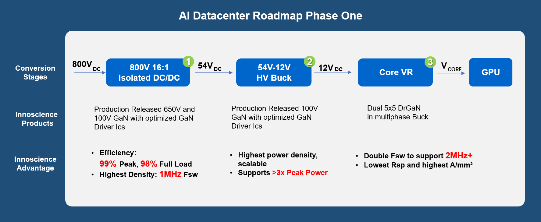
Beyond moving to 800V rack power, the architecture requires both ultra-high power density and ultra-high efficiency from 800V to 1V. Only gallium nitride power devices (GaN) are capable of simultaneously achieving these demanding requirements.
To meet the 800 VDC power density requirements, the power supply switching frequency must increase to nearly 1MHz, to shrink magnetics and capacitors size. Typical switching frequency in existing rack power supplies can reach 300kHz, but increasing to 1MHz yields approximately 50% reduction in magnetic core size.
Innoscience’s third-generation GaN provides decisive advantages:
(1)Compared to SiC on the 800V input side, Innoscience GaN reduces driver losses by 80% and reduces switching loss by 50% during each switching half-cycle, achieving a 10% decrease in overall power losses.
(2)On the 54V output side, only 16 Inno GaN devices are needed to achieve the same conduction loss as when 32 Si MOSFETs are used, doubling the power density and reducing the driving loss by 90%.
(3)Compared to Si FETs in existing rack architecture, 800 VDC low-voltage power conversion stage achieves 70% reduction in switching losses using GaN, and 40% increase in power output within same volume (increased power density).
(4)The GaN-based low-voltage power stage is scalable to support higher power GPU SKUs, and has improved dynamic response, also decreasing board capacitor cost.
As the industry’s only full-stack GaN supplier and the leading GaN IDM, Innoscience is the only company mass-producing GaN from 1200V to 15V, enabling a full conversion chain from 800V to 1V. This makes Innoscience the sole supplier capable of delivering an all-GaN power solution across all conversion stages, even as the architecture morphs in future for higher power.
Innoscience GaN also leads in reliability. Its third-generation devices have passed stringent accelerated stress tests, including extended 2000-hour dynamic HTOL, high-temperature (175°C) validation, and large-sample failure rate verification. Inline dynamic resistance monitoring and long-duration board-level stress testing ensure datacenter-grade lifetime performance exceeding 20 years.
As the world's leading GaN IDM, Innoscience's third-generation GaN devices offer exceptional fast switching, high efficiency, high power density, and superior reliability. With the integration of 800 VDC power architecture and Innoscience GaN technology AI datacenters will achieve the quantum leap from kilowatt racks to megawatt racks, ushering in an era of more efficient, higher performance, reliable, and greener AI accelerated computing.

 English
 简体
简体
