Battery Management Systems (BMS) are the central intelligence of modern energy storage, responsible for monitoring cell voltage, current, temperature, and other parameters to ensure safe and reliable charging and discharging. Often referred to as the “brain” of the battery system, a well-designed BMS is critical to achieving system longevity, performance, and safety.
According to the latest industry reports, approximately 43% of energy storage system failures are directly linked to BMS malfunction or functional limitations. At the core of BMS performance lies the power semiconductors that support protection, sensing, and switching.
As a global leader in GaN-on-Si technology, Innoscience has taken a pioneering role in bringing GaN into BMS applications. In 2022, through the collaboration with Oppo, Innoscience introduced 40V bi-directional VGaNTM that became the first GaN power device to be adopted in smartphones, marking a significant milestone for the industry. Since then, leveraging our proprietary 30V to 120V bi-directional GaN platform, Innoscience has introduced a portfolio of VGaNTM products, and complete BMS reference designs optimized for safety, thermal performance, and integration.

Bi-directional VGaNTM
Key Features of VGaN Technology for BMS Applications
- Bi-directional Conduction & Turn-off: Supports both forward and reverse current flow and switching in a single device, eliminating the need for back-to-back MOSFET configurations.
- Ultra-Low On-Resistance: Enables up to 40% reduction in charge/discharge power loss compared to conventional silicon MOSFETs, significantly reducing heat generation.
- Enhanced Robustness & SOA: High breakdown voltage, thermally stable threshold behavior, and favorable temperature coefficients contribute to a wider Safe Operating Area (SOA) and improved short-circuit resilience.
- Size & Weight Reduction: A single VGaNTM replaces two back-to-back Si MOSFETs, reducing solution size by over 30%. This is ideal for high-density battery systems such as drones, mobile devices, and compact medical equipment.
- System-Level Cost Optimization: Lower conduction and switching losses lead to simplified thermal management. Total system cost savings can exceed 20% due to reduced cooling and component count.
Target Applications
- Over-voltage protection (OVP)
- Battery pack switching and protection
- USB port protection in mobile devices
- High-side load switches in bi-directional converters
- Multi-power rail switching in embedded systems
VGaNTM BMS Solutions Offerings
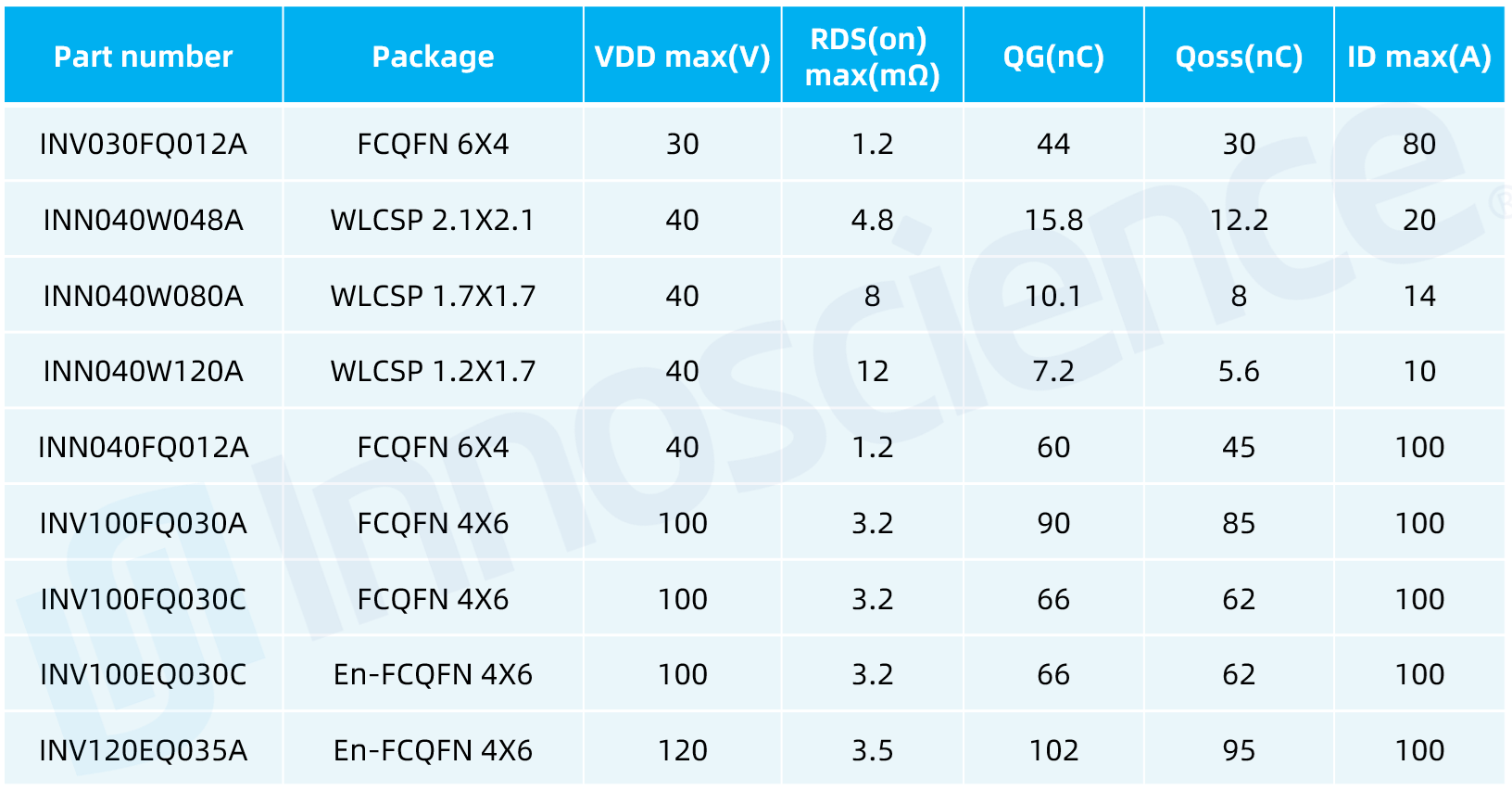
Design 1: INNDBMS120LS4
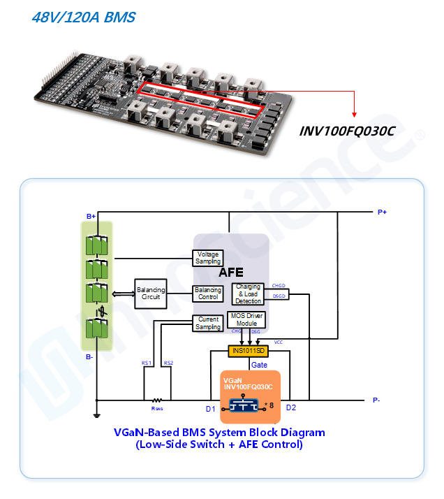
- GaN Solutions: INV100FQ030C*8 INS1011SD(VGaN Driver IC)
- Rated Current:120A
- Thermal Testing Results:82.9℃(100A@Ta=33℃/No airflow,no heatsink) 79.9℃(120A@Ta=32.2℃/no airflow,with heatsink)
Design 2:INNDBMS120HS3
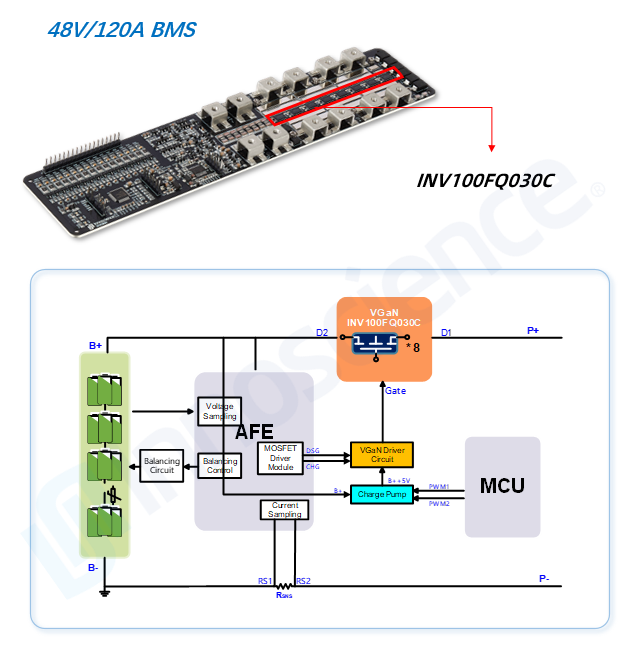
- GaN Solutions: INV100FQ030C*8
- Thermal Testing Results:63.9℃(100A@Ta=32.1℃/no airflow,no heatsink) 83.2℃(120A@Ta=36.3℃/ no airflow no heatsink)
Design 3:INNDBMS180HS1
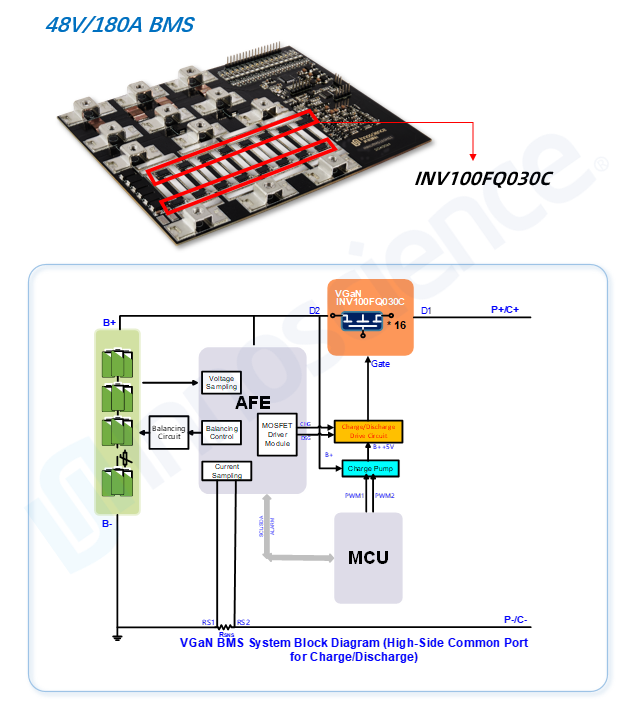
- GaN Solutions: INV100FQ030C*16
- Thermal Testing Results:73.9℃(150A@Ta=36.8℃/no airflow,no heatsink) 88.4℃(180A@Ta=38.4℃/ no airflow,no heatsink)
A Scalable GaN Solution for the BMS Ecosystem
Innoscience’s vertically integrated GaN platform, based on advanced 8-inch GaN-on-Si wafers, offers high integration, production scalability, and competitive cost structures. With its VGaNTM technology, Innoscience is well-positioned to serve the growing demands of automotive and energy storage BMS, offering customers reduced system size, lower thermal burden, and enhanced protection.
As the need for reliable BMS solutions in EVs, ESS, and portable electronics accelerates, Innoscience will continue to expand its portfolio with high-performance, application-ready GaN solutions that simplify design and accelerate time-to-market.
Learn More & Request Samples: Visit: www.innoscience.com
For technical inquiries: charlesbailley@innoscience.com

 English
 简体
简体
