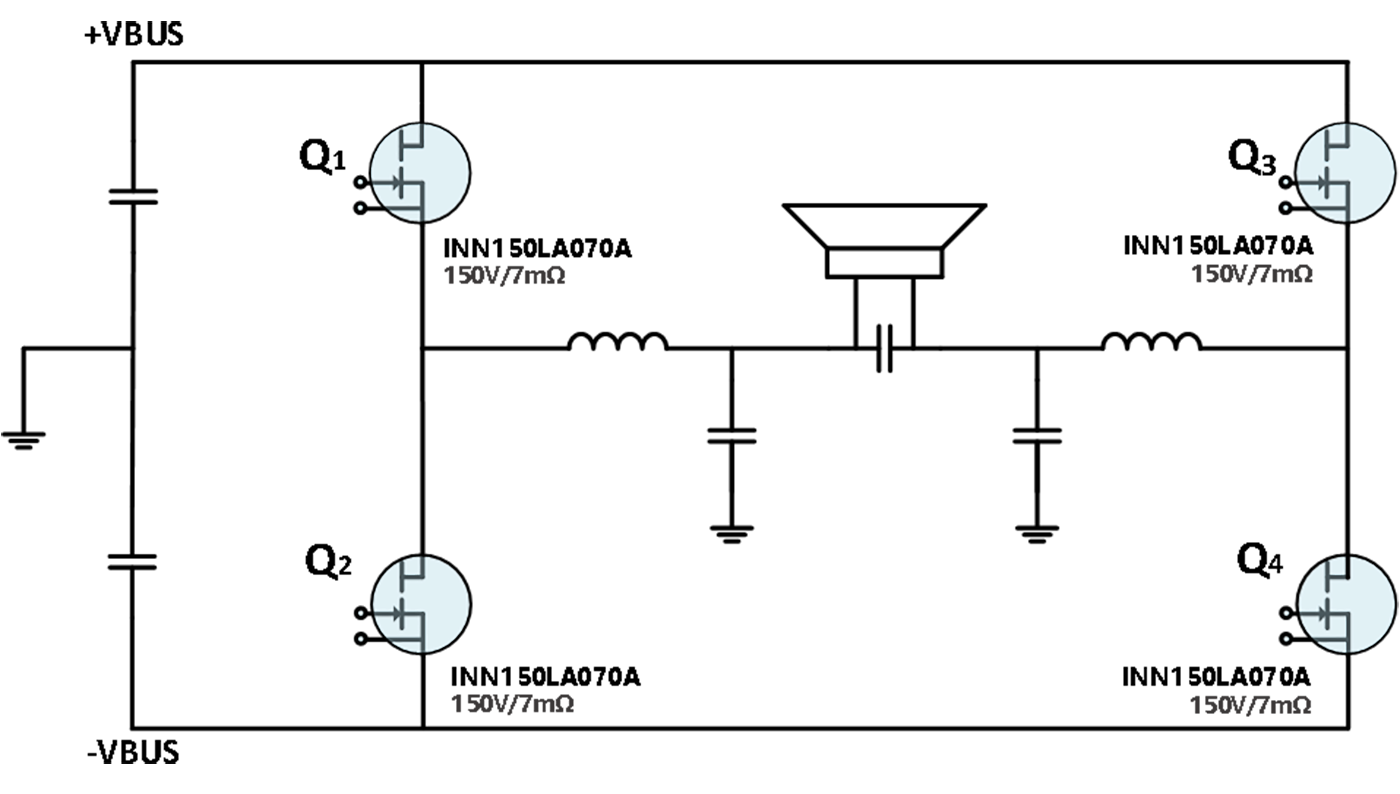
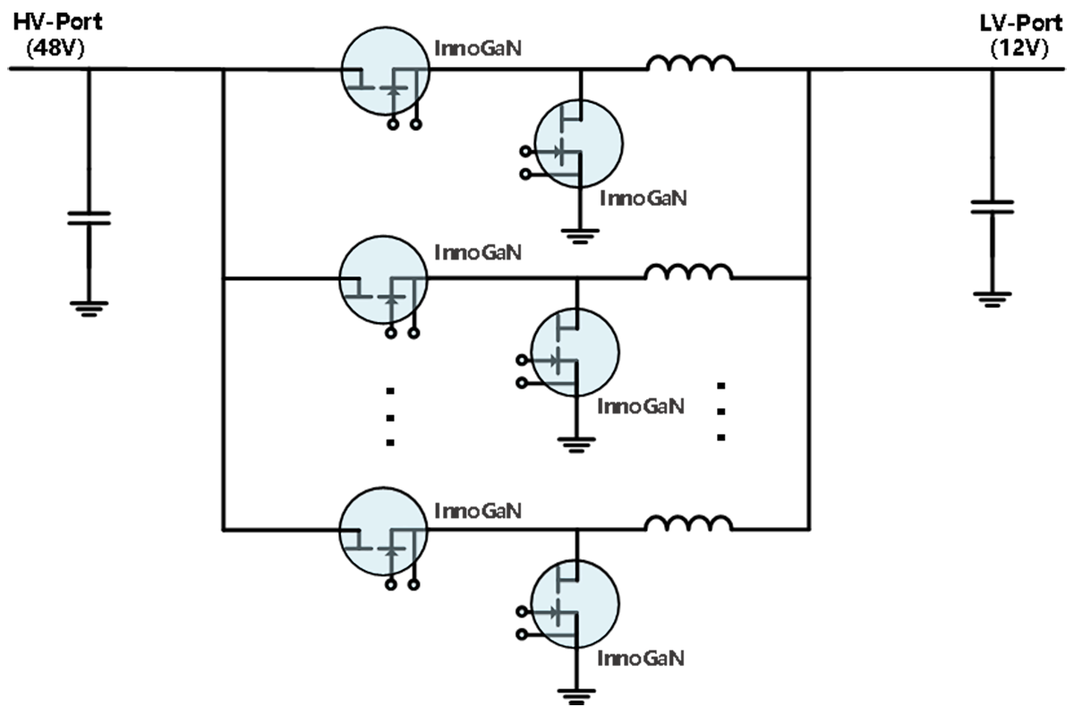
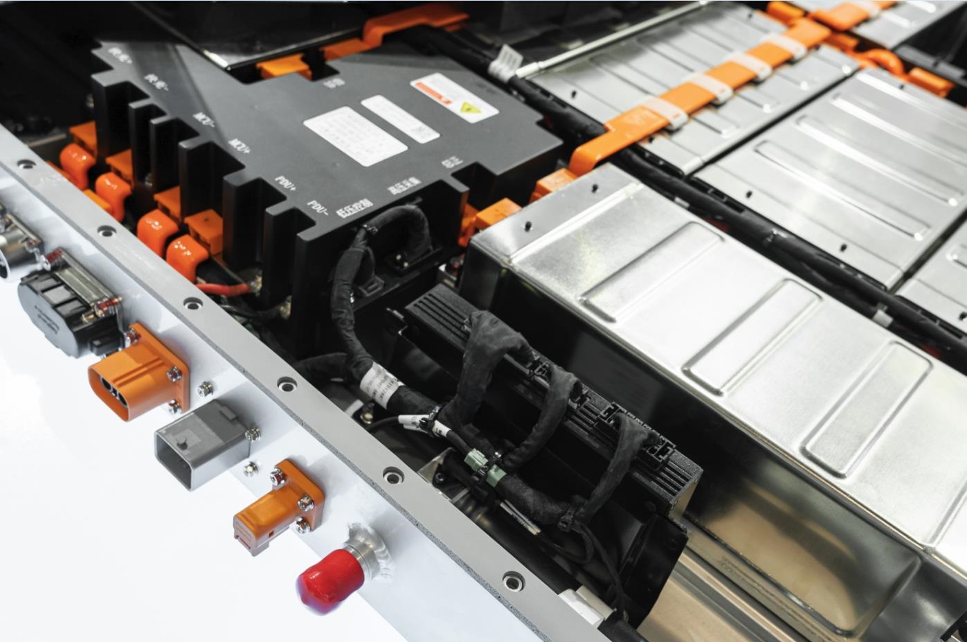
Consumer
  • Adapters

    Power Delivery (PD) chargers or adapter refers to small portable electronic power supply equipment.  It mainly converts AC input coming from the grid into (low voltage) DC output, and supplies power to small electronic products such as mobile phones, tablets, LCD monitors and notebook computers.

    Innoscience’s GaN technology enables adapters that are more powerful, much smaller and more efficient  than the one made with traditional Silicon technology.

    Description

    Today, our mobile phone are getting more and more powerful and there is a need to charge them faster and faster. Therefore, the power delivery (PD) chargers technology is evolving towards higher efficiency and higher power density, which allows adapters to be more powerful, and thus charge our phone faster, without increasing their size and wasting energy as heat. In order to achieve such objective, the adapter system needs to be more efficient and needs to operate at higher frequency that allow to use smaller passive components. The high frequency and high efficiency characteristics of Innoscience’s GaN technology meet these requirements enabling efficient and compact adapters. Several adapters (in-box and out-box) are already successfully using Innoscience’s GaN technology and sold in the consumer market.

    Compared with traditional Si MOSFET, GaN has the following advantages:
    1 Low Qg/Ciss: faster turn-on and turn-off, higher switching speed, reduce switching losses.
    2 Low Coss/Qoss: faster turn-on and turn-off and higher switching frequency, reduce switching losses.
    3 Qrr=0: No reverse recovery losses (absence of body diode), Reduce switching noise, better EMI performance.
    4 Low RDSON: reduce conduction losses.

    Solution topology view
    Main parameters of the scheme
    Scheme 1:SMPS——33W QR Flyback 
    Topology QR Flyback
    Input voltage 90-264Vac
    Output 3.3V~20V,11V/3A(max)
    Frequency 120KHz@230Vac
    Transformer ATQ1715,JPP95
    Efficiency 92.9% @230Vac & 20V/1.5A
    Size 26*26*26mm(PCBA)
    Watt density 30.8W/in3
    Device INN650DA04
    Control IC JW1515H+JW7726B
       
    Scheme 2:SMPS——65W QR Flyback 
    Topology QR flyback
    Input voltage 90-264Vac
    Output 20V/3.25A
    Frequency 135kHz @230Vac
    Transformer ATQ23.7,JPP95
    Efficiency 94.1% @230Vac & 20V/3.25A
    Size 48.7*27*26mm(PCBA)
    Watt density 31W/in3(PCBA)
    Device INN650DA260A
    Control IC NCP1342+MP6908A
       
    Scheme 3:SMPS——120W PFC+ACF 
    Topology Boost PFC+ACF
    Input voltage 90-264Vac
    Output 120W max
    ACF Frequency 230kHz @120W
    Transformer ATQ23,NVM02
    Efficiency 94.5% @230Vac & 20V/6A
    Size 46*46*26mm(PCBA)
    Watt density 35.7W/in3(PCBA)
    Device INN650D150A+INN650D260A*2
    Control IC NCP1622+JW1550
  • Wireless Charging

    Wireless charging refers to the magnetic field transfer of energy between the charger and the electric equipment, which can then be charged without the need of using wires.

    There are two types of wireless charging technologies: electromagnetic induction and coupled resonance. 

    Today, wireless charging technology is widely used in mobile phones, smart homes, electric car charging and other scenarios but their full potential is not yet fully exploited due to technology limitation.

    Innoscience’s GaN technology enables more powerful and efficient wireless charging systems thus unlocking the real potential of wireless charging technology and users to finally get rid of wires.

    Wireless Charging

    Compared to traditional Silicon technology, Innoscience’s GaN technology has the advantages of smaller parasitic capacitance, faster switching speed and smaller on-resistance per unit area. When applied to wireless charging system, Innoscience’s GaN technology reduces both the switching and conduction loss, thus enabling wireless charging system with higher system efficiency and longer transmission distance.

    Solution topology view
  • Class-D Audio Amplifier

    Class-D amplifiers based on Innoscience’s GaN technology enables audio systems that are smaller and provide a much higher sound quality to the user compared with what is possible with traditional technology. 

    Class-D Audio Amplifier

    The power loss of Class-D amplifier is much smaller than classical linear amplifier thanks to the fact that the Class-D amplifier operates in switching mode. This bring several benefits, which are among others: better sound quality, less heat, higher efficiency, smaller circuit board and thus smaller audio system, lower cost, extending battery life in portable systems etc… InnoGaNTM transistors area ideal for class-D amplifier by combining fast switching speed, low switching loss, small parasitic capacitance etc..

    The power transistor in Class-D amplifier operates in switching mode and generate a train of voltage pulses output. Thus, a low-pass filter is often inserted between the output stage and the speaker. Since most audio signals are not pulse trains, a modulator must be included in a Class-D amplifier to convert the audio input into pulses, so the pulses can drive the power transistor to operate. Since the Class-D amplifier operate in switching mode, the switching loss of the transistors become key for the system performance, which is why GaN technology is often used in Class-D amplifier for audio system. Compared to traditional Silicon transistors, InnoGaNTM transistors show: faster switching speed, lower switching loss, smaller parasitic capacitance (Coss) lower energy stored in output capacitance (Eoss), No reverse recovery losses (Qrr=0 thanks to the absence of the body diode). Moreover, lower switching loss enables to increase the pulse width modulation (PWM) frequency, which allow to reduce the size (and loss) of the low-pass filters. Furthermore, since Innoscience’s GaN (InnoGaNTM) devices switch fast, it is recommend to reduce the dead time of the PWM.

    Solution topology view
  • Over Voltage Protection (OVP)

    The Over Voltage Protection (OVP) unit function is to protect the main system by shutting down the unit

    when the input voltage exceeds a defined value.

    Nowadays, the USB type C port  is used not only for charging but on-the-go (OTG) or in reverse TX Mode.  Consequently and since the charging power of mobile phones are getting higher and higher, the battery protection circuits are nowadays indispensable. 

    Innoscience’s GaN technology enables efficient OVP systems and also the replacement of 2 Silicon MOSFETs with 1 GaN transistor. This saves on the overall OVP costs and makes the OVP unit smaller, which is very important considering the space constraints on mobile phone’s circuit boards.

    Over Voltage Protection (OVP)

    The Over Voltage Protection (OVP) unit function is to protect the main system by shutting down the unit when the input voltage exceeds a defined value. The size of each unit inside a mobile phone or laptop is of paramount importance and InnoGaNTM transistors enable the OVP unit to be 50% smaller than the one made with Silicon technology. This is achieved by replacing two MOSFET devices with one InnoGaNTM bi-directional transistor. Indeed, thanks to the absence of the body diode, InnoGaNTM realizes the bidirectional shutdown on its own. At the same time, the overall system losses are reduced thanks to the lower on-resistance of InnoGaNTM devices compared to Silicon MOSFET. This increases the charging efficiency and produce less heat.

    Solution topology view
    Main parameters of the scheme
    Bi-GaN  
    Part Number INN40W08
    Configuration Single
    VDD(Max)/V 40
    ID( continous current , max)/A 15
    RDD(on)(type)/mOhm 5.5
    Package(mm) 2X2
  • Time of Flight (ToF)

    Time of Flight (ToF) is a method to measure distance and map 3D space accurately by measuring the time that is needed for an optical signal, which is generated by a laser, to be reflected back to the system source.

    Some of Light Detection and Ranging (LIDAR) system are based on ToF methods and there are used in the latest generations of mobile phone (flash LIDAR), they are key for AR/VR devices as well as they are used in surveillance and automotive for safety sensor as well as for self driving experience (often scanning LIDAR).

    Innoscience’s GaN technology is used today as driver for the lasers inside LIDAR systems. By providing shorter and faster pulses, Innoscience’s GaN technology enables LIDAR systems that have higher resolution and longer range with respect to what is possible with traditional Silicon technology.

    Time-of-flight (ToF)

    The resolution and measure distance in LIDAR systems based on Time-of-flight (ToF) is determined by the laser driver of the system. InnoGaNTM transistors are today used in ToF applications to drive the laser as they provide simultaneously higher current (i.e. longer measure distance) and narrower pulse width (i.e. higher resolution) compared to traditional Silicon technology. Therefore, Innoscience’s GaN Technology with smaller area cost and higher performance is a better choice for ToF system.

    Solution topology view
Industrial
  • Motor Driver and Control

    Permanent magnet motor refers to a kind of electromagnetic device based on the Faraday law of electromagnetic induction to achieve electric energy conversion or transfer. The main role is to generate driving torque, as the power source of electrical appliances or various machinery.  Motors are widely used in consumer electronics, household appliances, industrial manufacturing, robotic and other fields.

    InnoGaNTM enables motor driver and inverters to be smaller, lighter, cheaper, more reliable and efficient with respect to what is possible today with Silicon technology. 

    Motor Driver and Control

    Silicon technology has difficult to catch up with the increase need of higher power density as the one required by motor drivers or inverters for e.g. DC brushless motors. Compared to traditional Silicon technology, InnoGaNTM devices have lower switching loss and no reverse recovery current thanks to the absence of the body diode. Thanks to these properties, with InnoGaNTM is possible to increase the PWM frequency to a level that the input filter of the inverter can be substituted by a simple inexpensive ceramic capacitor, which are also overall more reliable then traditional electrolytic capacitors. This results in smaller, lighter, cheaper, more reliable and efficient motor driver with respect to what is possible today with Silicon technology.

    Solution topology view
  • Telecom Infrastructure

    Communication base stations are an essential element of our networks as they are the interface for mobile devices to access Internet. 

    With the popularization of 5G, there is a need of having a large network of (mini) base stations to better serve customers and provide the needed bandwidth.

    It has been calculated that 5G base stations consumes significant more energy than 4G base stations. Therefore, there is a strong need to equip them with highly efficient and reliable power supply as the one enabled by InnoGaNTM.

    Telecom infrastructure

    With the rapid development of 5G, consumers will get higher bandwidth, lower latency and more advanced services. Unfortunately, this will result in a dramatic increase of the power consumption of base stations.  InnoGaNTM enables highly efficient and small volume power supply systems for 5G base station and thus lower their power consumption. This is thanks to the inherent property of InnoGaNTM device, such as small parasitic capacitance, fast switching speed and small static and dynamic losses.

    Solution topology view
  • LED Lighting

    Under the general trend of low-carbon and green development, LED lighting are spreading very rapidly.  In addition to traditional lighting application fields, other application fields such as smart lamp poles, plant lighting and other emerging applications based on LED are increasing day-by-day.

    InnoGaNTM enables drives for LED that are smaller, thinner and much more efficient than traditional drivers made with Silicon technology.

    LED lightning

    Traditional Silicon LED driver for mid- and high-power LED are bulky, complex and costly. InnoGaNTM switching speed is more than 8 times faster than traditional silicon FET and switching loss can be reduced up to 70%. Moreover, since the gate charge (Qg) characteristic of InnoGaNTM is 1/12 of the one of Silicon device, LED driver based on InnoGaNTM technology can have a 90% reduction of the driver losses when switching at higher frequency (e.g. 400KHz). Furthermore, thanks to the absence of the body diode, InnoGaNTM devices have no reverse recovery loss and this results in better EMI performance. This means that InnoGaN technology does not need a capacitor to reduce EMI as is often done with Silicon technology, thus saving in cost and additional source of loss. LED drivers powered by InnoGaNTM devices show smaller switching conduction losses, higher efficiency, higher switching frequency and an overall reduction of the driver size that becomes much smaller and thinner than what would be possible with Silicon technology.

    Solution topology view
    Main parameters of the scheme
    200W/(LED Driver)  
    Topology Boost PFC+LLC
    Input voltage range 180-264Vac
    Output 47~49V,CC 4.2A,TYP 48V
    LLC working frequency 300kHz @Full load
    Transformer ER25/12,TP5
    Efficiency 96% @230Vac & CC4.2A 48V
    Size 196*35*13 mm(PCBA)
    Power density 35W/in3(PCBA)
    Application products INN650D150A+INN650D260A*2
  • Photovoltaic and Energy Storage System

    From small to big solar panel installations, InnoGaNTM can overall improve the efficiency of the PV system. InnoGaNTM plays a key role in increasing the efficiency, reducing the size and bill-of-material of (micro-) inverters, auxiliary power supply and on the maximum power point tracker (MPPT), which is needed to maximize the cell power output and thus get the best out the PV cells.

    Moreover, more and more solar panel installations are equipped with an energy storage system that allow storing energy for then utilize it later. InnoGaNTM enables systems with low loss of energy transfer and high efficiency of energy conversion.

    Photovoltaic and Energy Storage System

    Green energy source such as Photovoltaic (PV) systems are nowadays widely used to achieve low-carbon emission and green development. Possibly, such a source of energy needs also to be combined with appropriate energy storage systems for an appropriate energy utilization also during the dark hours. Thanks to the inherent property of InnoGaNTM device, such as low static and dynamic losses, small parasitic capacitance, fast switching speed, high frequency capabilities etc.. InnoGaNTM can effectively increase the efficiency of (micro-) inverters, auxiliary power supply and on the maximum power point tracker (MPPT). Next to this, the power conversion system switches at higher frequencies and produce cleaner sine wave. This results in a significant reduction of the passive components and thus an overall size, weight and cost reduction of the overall system, which also becomes more reliable by getting rid of electrolytic capacitors. Moreover, for the same reasons, InnoGaNTM enables energy storage conversion systems to achieve low energy transfer loss and highly efficient energy conversion.

    Solution topology view
  • Data Center

    InnoGaNTM devices significantly increase the efficiency of power conversion systems inside data centers. According to Energy Innovation, a 1 percent improvement translates into an overall reduction of 1 megawatt per data center!

    InnoGaNTM plays a key role in increasing the efficiency and reducing the size of each power conversion stage of a power supply rack. They enable more compact, more efficient and reliable power conversion systems for data centers. 

    Data Center

    Data centers waste a lot of energy in their energy conversion systems and we will need hundreds of nuclear reactors just to run data centers. InnoGaNTM plays a key role in increasing the efficiency and reducing the size of each power conversion stage of a power supply rack. For instance, InnoGaNTM devices reduce the size and increase the efficiency of traditional 48V to 12V or 5V power conversion and also enable 48V to 1V direct power conversion. The latter is very important as it allows to eliminate the multi stages that are needed when using traditional Silicon technology. Power conversion systems based on Innoscience’s GaN technology are overall more efficient and thus consume less energy that means less pollution and lower energy bill. They are also more compact and reliable thanks to the high frequency capabilities of InnoGaNTM devices that allow shrinking of the passive components (thus leaving more space for computational units) and also the usage of ceramic capacitors instead of traditional electrolytic capacitors, which are more prone to failures.

    Solution topology view
    Main parameters of the scheme
    300W LLC  
    Topology LLC
    Input voltage range 36-60V
    Output 300W
    ACF working frequency 915kHz
    Efficiency 97%(Peak value) 95.5%(300W)
    Size 27mm*18mm*6mm
    Power density 1700W/in3
    Application products INN100W12*4
    Control scheme UCD3138
Automotive
  • On-Board Charger (OBC)

    On-board charger (OBC) converts alternative current (AC), as the one coming from the grid, into a direct DC voltage that is used to charge the battery pack.

    InnoGaNTM devices enable highly efficient, compact, lightweight and reliable OBC systems.

    On-Board Charge (OBC)

    OBC is the core component of electric vehicles as it converters the AC current coming from the grid into DC voltage that is needed to charge the battery. The OBC efficiency has a significant impact on the charging speed of the electric vehicle: an OBC with higher efficiency results in an overall reduction of the charging time. Next to this, there is a need to increase the overall power density of OBC systems, as this means smaller and lighter systems, which has lower impact on the total weight of the vehicle (i.e. longer range). Automotive companies have already realized that the efficiency and power density of OBCs made with traditional Silicon power device have reached the upper limit.  Thanks to the inherent property of InnoGaNTM device, such as small parasitic capacitance, fast switching speed, high frequency capabilities and small static and dynamic losses, it is possible to make OBC systems more efficient. Moreover, by operating the OBC system at higher switching frequency, it is possible to shrink the passive components and thus obtain more compact and lighter systems. To add on this, the higher frequency operation would also enable the usage of small and reliable ceramic capacitors (instead of conventional and bulky electrolytic capacitors more prone to failure).

    Solution topology view
  • 48V Power System

    There is a trend in the automotive industry to move from traditional 12V to a 48V power systems in order to increase power delivery and reduce resistive loss.

    There is a strong need to improve the efficiency of the 48V bidirectional DC-DC converter as well as to make them smaller and lighter.

    Thanks to the high frequency capabilities of InnoGaNTM devices and their low static and dynamic losses, InnoGaNTM technology enables more reliable, compact and lightweight 48V DC-DC converters for automotive applications. 

    48V Power System

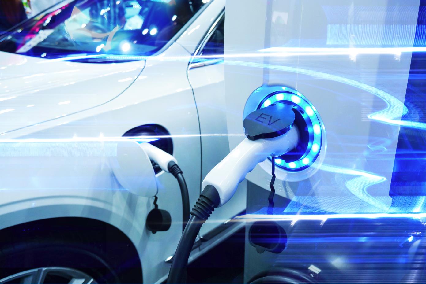
    Cars are offering more and more interactive functions, displays, sensors etc.. to their users. Therefore, there are more and more electronic devices to be powered inside the car and this demands for an efficient power distribution system. For this reason, the automotive industry is switching from 12V bus to a more efficient 48 V bus power distribution. 
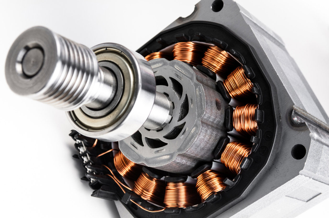
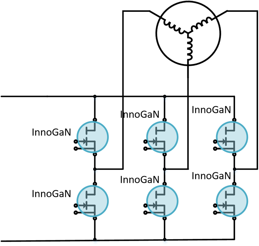
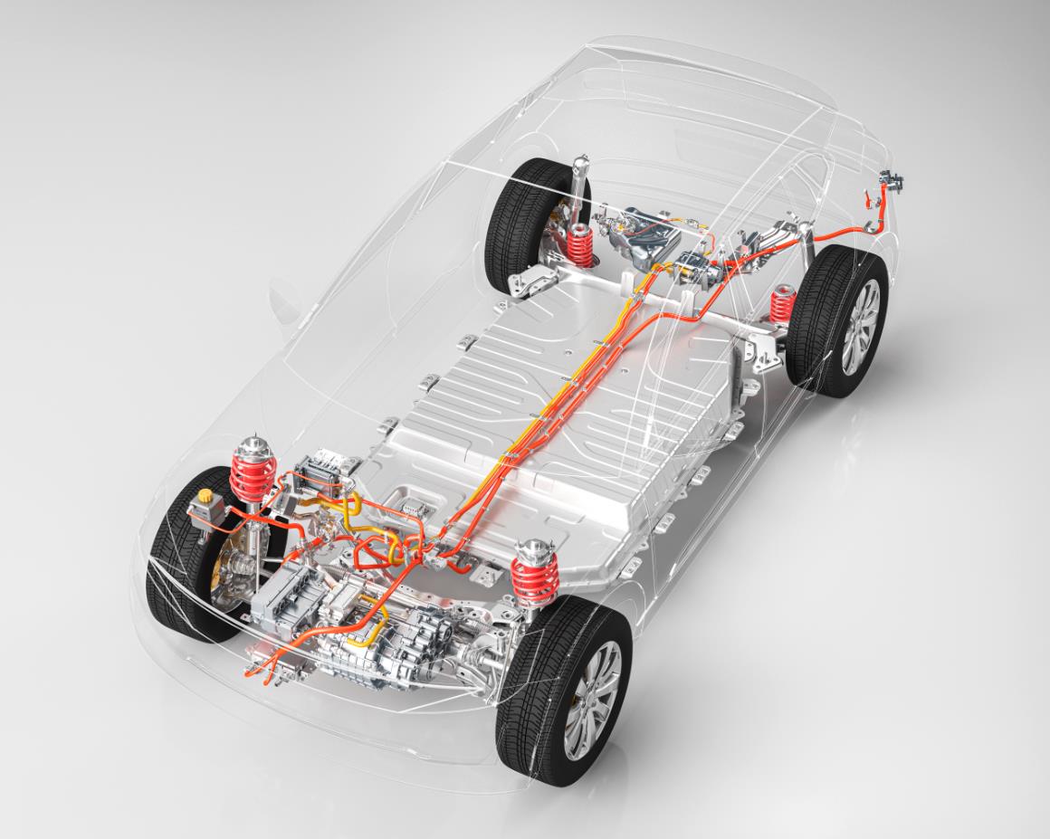
The 48V system is mainly composed of three parts: 48V battery pack, Belt-Driven Starter Generator (BSG) motor, and 12V/48V bidirectional DC-DC converter. The 48V power system supplies power to the on-board system and, at the same time, it is used for the automatic start and stop functions of the vehicle. The 48V power system is also responsible for the kinetic energy recovery function. 
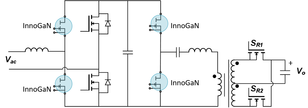
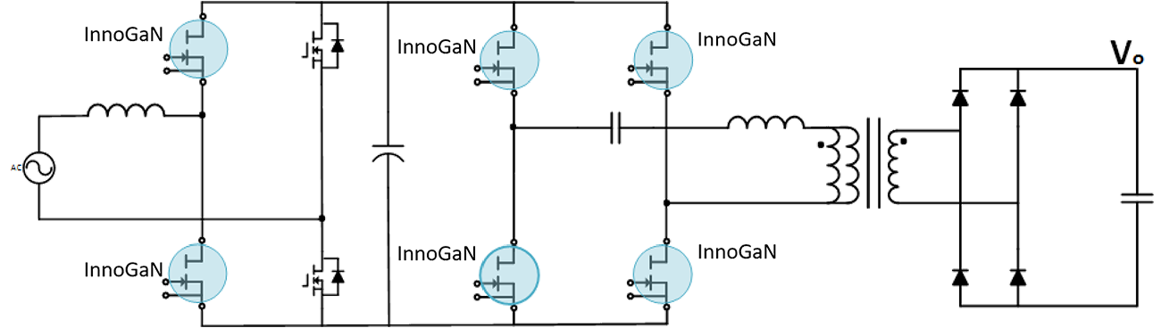
Such 48V power distribution system requires highly efficient, compact and lightweight 48V DC-DC converter. Thanks to the excellent switching characteristics and high frequency capabilities of InnoGaNTM , which is at least a factor 2 higher than Silicon, it is possible to make 48V DC-DC converters smaller and lighter, by shrining the passive components, as well as to make them more efficient by reducing the loss related to inductors. This is combined with the low static and dynamic losses of InnoGaNTM devices, which result in an overall lower loss of the whole 48V converter. Moreover, by switching at high frequency, it is possible to move from conventional electrolytic capacitors to smaller and more reliable ceramic capacitors that make the overall 48V power system more reliable.

    Solution topology view
  • Battery Management System (BMS)

    The battery management system (BMS) is a system to ensure safe charging and discharging as well as to prevent damage and failures of the vehicle’s battery pack. The BMS is normally equipped with a battery protection unit (BPU) that disconnects the battery from the charger or load when needed.

    Thanks to the fact that InnoGaNTM devices do not have a body diode, it is easy to replace the two Silicon NMOS, today used in standard BPU, by one InnoGaNTM.This saves in costs and makes the system overall simpler and more efficient. 

    Battery Management System (BMS)

    Nowadays, the Lithium-Ion batteries are widely used thanks to their high power density. Unfortunately, however, the Lithium-Ion batteries  are also unstable when the batteries work at critical conditions such as  over-charging/discharging, high/low Temperatures, over-current/voltage etc.. Therefore, the BMS is normally equipped with a battery protection unit (BPU) that disconnects the battery from the charger or load when the system sense abnormal state. The BPU usually is formed by two back-to-back Silicon NMOS (common source or common drain) for charging and discharging. Thanks to the fact that InnoGaNTM devices do not have a body diode, it is easy to replace the two NMOS by one InnoGaNTM , which has overall lower static and dynamic losses. This saves in costs and makes the system overall simpler, more reliable and efficient.

    Solution topology view
  • Time of Flight (ToF)

    Time of Flight (ToF) is a method to measure distance and map 3D space accurately by measuring the time that is needed for an optical signal, which is generated by a laser, to be reflected back to the system source.

    Some of Light Detection and Ranging (LIDAR) system are based on ToF methods and there are used in the latest generations of mobile phone (flash LIDAR), they are key for AR/VR devices as well as they are used in surveillance and automotive for safety sensor as well as for self driving experience (often scanning LIDAR).

    Innoscience’s GaN technology is used today as driver for the lasers inside LIDAR systems. By providing shorter and faster pulses, Innoscience’s GaN technology enables LIDAR systems that have higher resolution and longer range with respect to what is possible with traditional Silicon technology.

    Time-of-flight (ToF)

    The resolution and measure distance in LIDAR systems based on Time-of-flight (ToF) is determined by the laser driver of the system. InnoGaNTM transistors are today used in ToF applications to drive the laser as they provide simultaneously higher current (i.e. longer measure distance) and narrower pulse width (i.e. higher resolution) compared to traditional Silicon technology. Therefore, Innoscience’s GaN Technology with smaller area cost and higher performance is a better choice for ToF system.

    Solution topology view
Login