English
 中文
中文

1.1 Features
- Bi-directional blocking capability
- GaN-on-Silicon E-mode HEMT technology
- Ultra-low on resistance
40V Bi-directional GaN Enhancement-mode Power Transistor
Bi-directional GaN-on-Silicon enhancement mode high-electron-mobility-transistor (HEMT) in FCQFN with 6 mm x 4 mm package size.
| Platform (B040E2.5) | ||||
|---|---|---|---|---|
| Product (INN040FQ012A) | ||||
| Test Items | Test Conditions | Sample Size (Unit x Lot) | #Fail | Result |
| HTRB | T=125°C, VD1=32V, 168hrs | 77 x 1 | 0 Fail | Pass |
| HTRB | T=125°C, VD2=32V, 168hrs | 77 x 1 | 0 Fail | Pass |
| HTGB | T=125°C, VG=5.5V, 168hrs | 77 x 1 | 0 Fail | Pass |
| MSL3 | T=30°C, RH=60%, 3 x reflow, 192hrs | 25 x 2 | 0 Fail | Pass |
| TC | -40 to +125°C, Air, 1000Cys | 77 x 3 | 0 Fail | Pass |
| H3TRB | T=85°C, RH=85%, VD1=32V, 1000hrs | 77 x 3 | 0 Fail | Pass |
| H3TRB | T=85°C, RH=85%, VD2=32V, 1000hrs | 77 x 3 | 0 Fail | Pass |
| HTSL | T=150°C, 1000hrs | 77 x 3 | 0 Fail | Pass |
| Drop test |
Accelerometer: 1500G Durations: 0.5ms, 90Drops |
77 x 1 | 0 Fail | Pass |
| Solderability | Pre-Con: 8hrs Pb-free: 245±5°C, 5±0.5s |
25 x 3 | 0 Fail | Pass |
| HTOL | Tj=125°C, Load current, 168hrs | 8 x 1 | 0 Fail | Pass |
| HBM | All Pins | 3 x 1 | 0 Fail | Pass |
| CDM | All Pins | 3 x 1 | 0 Fail | Pass |
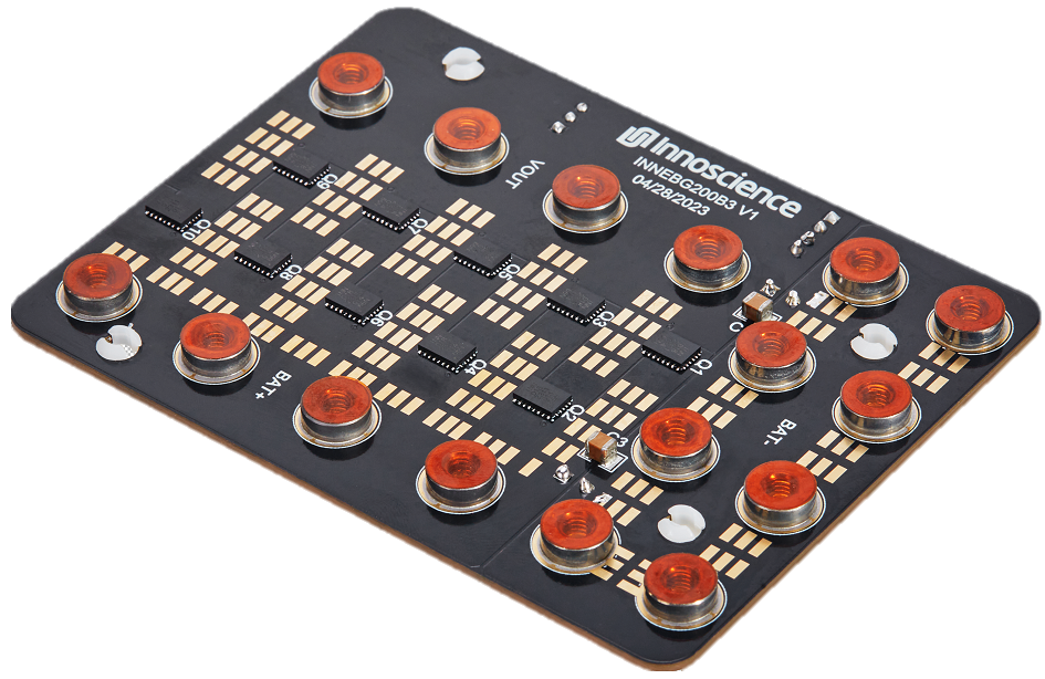
Small size: L105mm*D80mm*H18mm
High current capability:200A
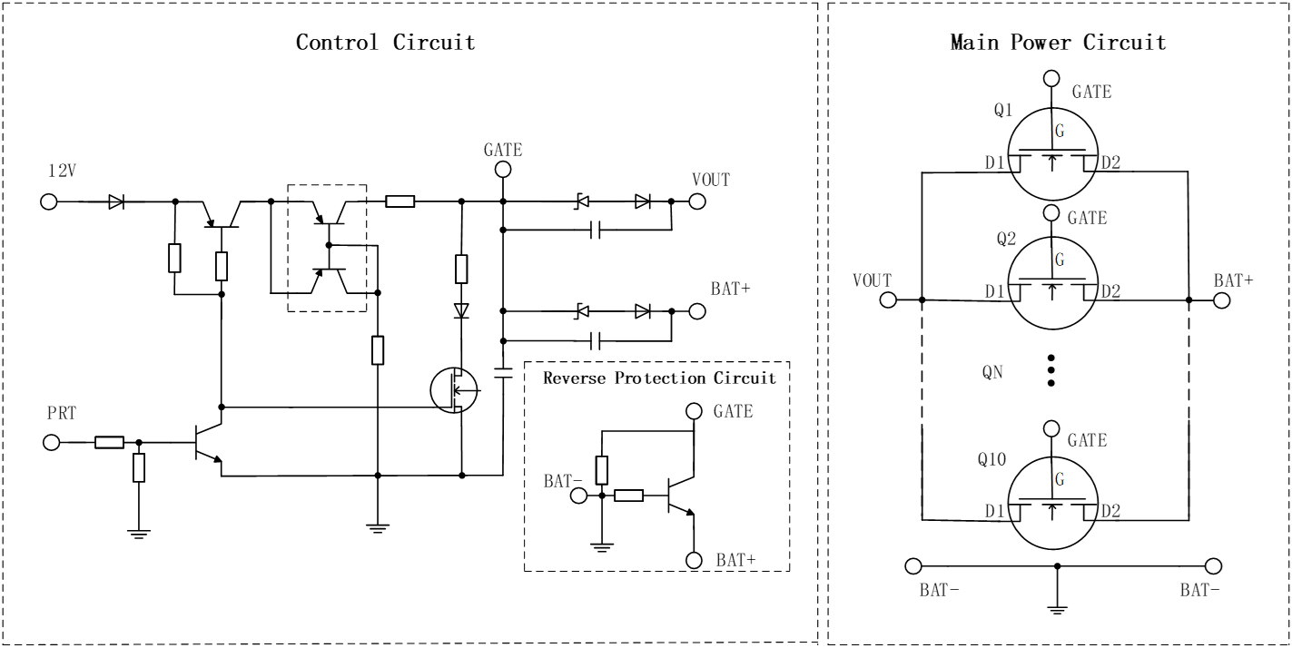
Simple structure and convenient control: PRT (low: off; high: on)
Low temperature rise: 25.3℃(200A@Ta=25℃,2.5m/s airflow,10pcs in parallel)
Battery reverse connection protection function
Load Switch
| Parameter | Value |
|---|---|
| VDD,max | 40V |
| RDD(on),max @ VG = 5 V | 1.2mΩ |
| QG,typ @ VDD = 20 V | 60nC |
| ID,DC | 100A |