 English
 中文
中文

1.1 Features
- Bi-directional blocking capability
- GaN-on-Silicon E-mode HEMT technology
- Ultra-low on Resistance
40V VGaN Enhancement-mode FET
Bi-directional GaN-on-Silicon enhancement mode high-electron-mobility-transistor(HEMT) based on advanced low voltage BiGaN Technology with ultra-low on resistance.
Innoscience’s E-mode GaNFETs were subjected to a variety of reliability test under the condition referenced to typical for silicon-based power MOSFETs.These test items and results were shown as below:
| Platform (B040E2.5) | ||||
|---|---|---|---|---|
| Product (INN040W048A) | ||||
| Test Items | Test Conditions | Sample Size (Unit x Lot) | #Fail | Result |
| MSL1 | T=85°C, RH=85%, 3 x reflow, 168hrs | 25 x 2 | 0 Fail | Pass |
| HTRB | T=125°C, VD1=32V, 1000hrs | 77 x 3 | 0 Fail | Pass |
| HTRB | T=125°C, VD2=32V, 1000hrs | 77 x 3 | 0 Fail | Pass |
| HTGB | T=125°C, VG=5.5V, 1000hrs | 77 x 3 | 0 Fail | Pass |
| TC | -40 to +125°C, Air, 1000Cys | 77 x 3 | 0 Fail | Pass |
| H3TRB | T=85°C, RH=85%, VD1=32V, 1000hrs | 77 x 3 | 0 Fail | Pass |
| H3TRB | T=85°C, RH=85%, VD2=32V, 1000hrs | 77 x 3 | 0 Fail | Pass |
| HTSL | T=150°C, 1000hrs | 77 x 3 | 0 Fail | Pass |
| HTOL | Tj=125°C, Load current=7A, 1000hrs | 32 x 3 | 0 Fail | Pass |
| Drop test |
Accelerometer: 1500G Durations: 0.5ms, 90Drops |
77 x 1 | 0 Fail | Pass |
| Solderability | Pre-Con: 8hrs Pb-free: 245±5°C, 5±0.5s |
25 x 3 | 0 Fail | Pass |
| HBM | All Pins | 3 x 1 | 0 Fail | Class 1B |
| CDM | All Pins | 3 x 1 | 0 Fail | Class C2b |
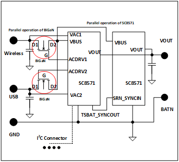
Vin:8~22V
Controller IC:SC8571
Iomax:14A
Bi-directional switch
OVP Application
OCP Application
| Parameter | Value |
|---|---|
| VDD,max | 40V |
| RDD(on),max @ VG = 5 V | 4.8mΩ |
| QG,typ @ VDD = 20 V | 15.8nC |
| ID,DC | 20A |

.png)