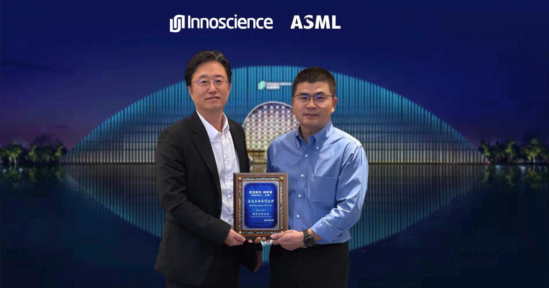
Innoscience Technology (Zhuhai) Co., Ltd. (“Innoscience”) recently held a ceremony to celebrate the introduction of the lithography scanner for manufacturing Innoscience’s 8-inch Gallium Nitride on Silicon (GaN-on-Si) wafers for power switching applications. In 2021, Innoscience introduced the lithography scanner from ASML. Thanks to the excellent imaging performance and unique dual-stage TWINSCAN architecture of ASML’s lithography scanner, the productivity and line yieldof Innoscience GaN-on-Si power devices are improved. During the ceremony, Shen Bo, ASML Vice President and China Country General Manager, was awarded the "Best Strategic Partner" by Innoscience on behalf of ASML.
The “third-generation semiconductors”, such as Gallium Nitride (GaN) and Silicon Carbide (SiC), have been in the spotlight of the global semiconductor industry in recent years, characterized by their smaller size, higher switching frequencies capabilities, higher efficient energy management with higher power densities than what is possible with traditional Silicon material. Such new materials can fulfill the global strategic needs such as energy-saving, emission reduction, smart manufacturing, etc. GaN is one of the key "third-generation semiconductor" materials, which has broad market prospects and can penetrate a wide range of applications covering consumers, industrials and automotive. As the world's leading 8-inch GaN-on-Si Integrated Device Manufacturer (IDM), Innoscience is committed to promoting innovation and revolution of the third-generation semiconductor manufacturing technology.
“We introduced ASML's lithography scanner in the second quarter of this year, which has enhanced our lithography process window, line yield, productivity, and cost-efficiency. After the scanner move-in, ASML's customer service team and our engineers efficiently overcame the technical challenges through on-site verification and iterationto successfully achieve trial production within only three months, and eventually entered the formal mass production stage in October. By working with ASML, the world’s leading supplier in the semiconductor industry, Innoscience’s production process has been streamlined and accelerated to support the booming GaN semiconductor industry,” said Jay Son, CEO of Innoscience.
This is also the first time ASML's lithography system has made a breakthrough into the global mass production of 8-inch GaN-on-Si power semiconductor wafers. To better support Innoscience, ASML has been upgrading the lithography scanner according to Innoscience’s manufacturing requirements. The successful introduction of ASML lithography scanner will continue to facilitate the mass production of Innoscience's GaN-on-Si power semiconductor devices and to contribute to its long-term development.
"We are proud to be a partner of Innoscience and honored of receiving such award. The booming growth of Innoscience reflects the development and long-term potential of the third-generation semiconductor industry," said Shen Bo, "ASML has assiduously supported and served customers with our leading lithography technology to drive the innovation in semiconductor industry. We will continue to provide advanced technology and excellent services to support the long-term development of Innoscience.”
Ron Kool, Executive Vice President of DUV Business Line said, “We are proud to see the superior performance of ASML TWINSCAN lithography is verified for the first time in the field of 8-inch GaN-on-Si power semiconductor wafers. We are fully confident to support Innoscience's continued growth in the future."
About Innoscience
Innoscience is an Integrated Device Manufacturer (IDM) founded in December 2015 with investment from venture capitals from the world. With the development of new technologies, the electric power grid and power electronic systems across the world are undergoing a massive transformation. Our vision is to create an energy ecosystem with effective and low-cost Gallium-Nitride-on-Silicon (GaN-on-Si) power solutions. In November 2017, Innoscience first established a mass production 8-inch wafer line for GaN-on-Si devices. As a cutting-edge GaN technology provider, Innoscience’s 1,400+ employees and over 300 R&D experts are dedicated to delivering high performance and high reliability GaN power devices that can be widely used in diverse applications including cloud computing, electric vehicles (EV) and automotive, portable devices, mobile phones, chargers and adapters. For more information, please visit www.innoscience.com.
About ASML
ASML is a leading supplier to the semiconductor industry. The company provides chipmakers with hardware, software and services to mass produce the patterns of integrated circuits (microchips). Together with its partners, ASML drives the advancement of more affordable, more powerful, more energy-efficient microchips. ASML enables groundbreaking technology to solve some of humanity's toughest challenges, such as in healthcare, energy use and conservation, mobility and agriculture. ASML is a multinational company headquartered in Veldhoven, the Netherlands, with offices across Europe, the US and Asia. Every day, ASML’s more than 30,000 employees (FTE) challenge the status quo and push technology to new limits. ASML is traded on Euronext Amsterdam and NASDAQ under the symbol ASML.
Discover ASML – our products, technology and career opportunities – at www.asml.com
原文链接:https://www.laoyaoba.com/n/800649

 English
 中文
中文
